Circuit component, electrode connection structure and display device including the same

a technology of electrode connection and circuit component, which is applied in the direction of electrical apparatus construction details, instruments, casings/cabinets/drawers, etc., can solve the problems of low adhesion of the second circuit component to the plastic plate of the first circuit component, and the likelihood of cracking in the barrier film below the terminals. , to achieve the effect of reducing the damage to the electrode, reducing

Inactive Publication Date: 2011-06-07
SHARP KK
View PDF15 Cites 4 Cited by
  • Summary
  • Abstract
  • Description
  • Claims
  • Application Information

AI Technical Summary

Benefits of technology

[0019]In order to overcome the problems described above, preferred embodiments of the present invention reduce the damage to the electrodes by reducing the propagation of the crack in the barrier film and improve the adhesion between the circuit components.

Problems solved by technology

Therefore, a crack is likely to occur in the barrier film below the terminals.
If the material of the terminals and the size and material of the conductive particles are varied, the technique of Japanese Unexamined Patent Publication No. 2001-337340 may not work enough to reduce the damage to the terminals of the first circuit component caused in the press bonding of the second circuit component and the electrical connection may not be maintained in good condition.
The problem also arises in the cases where the ACF is not provided (i.e., the terminals are directly press bonded), where the ACF is replaced with conductive paste, an NCF (non conductive film) or an adhesive resin, and where common transfer electrodes are interposed between the electrodes.
Further, due to low adhesion of the barrier film to the plastic plate, there is also a problem of low adhesion of the second circuit component to the plastic plate of the first circuit component.

Method used


Image

  • Circuit component, electrode connection structure and display device including the same
  • Circuit component, electrode connection structure and display device including the same
  • Circuit component, electrode connection structure and display device including the same

Examples


first preferred embodiment

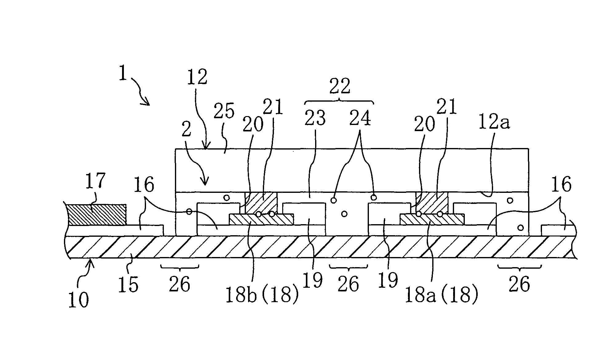
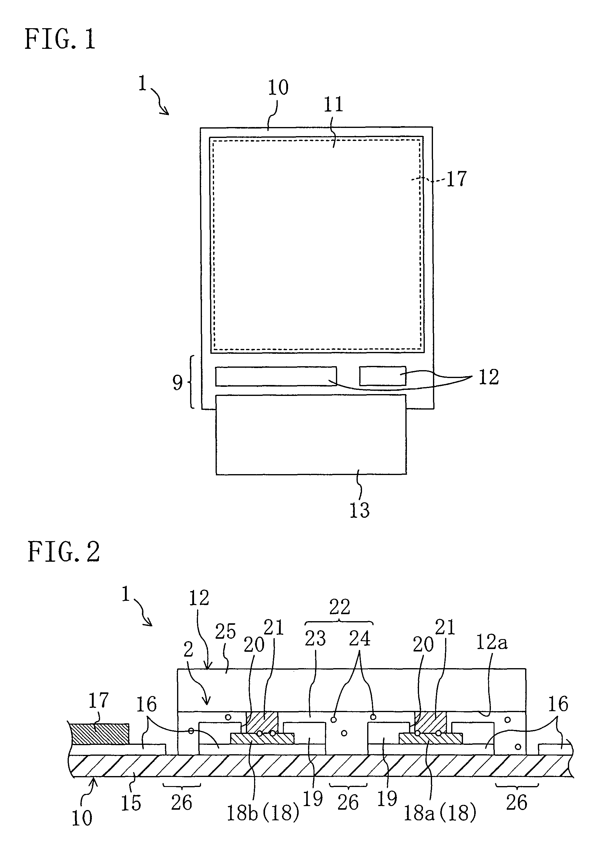
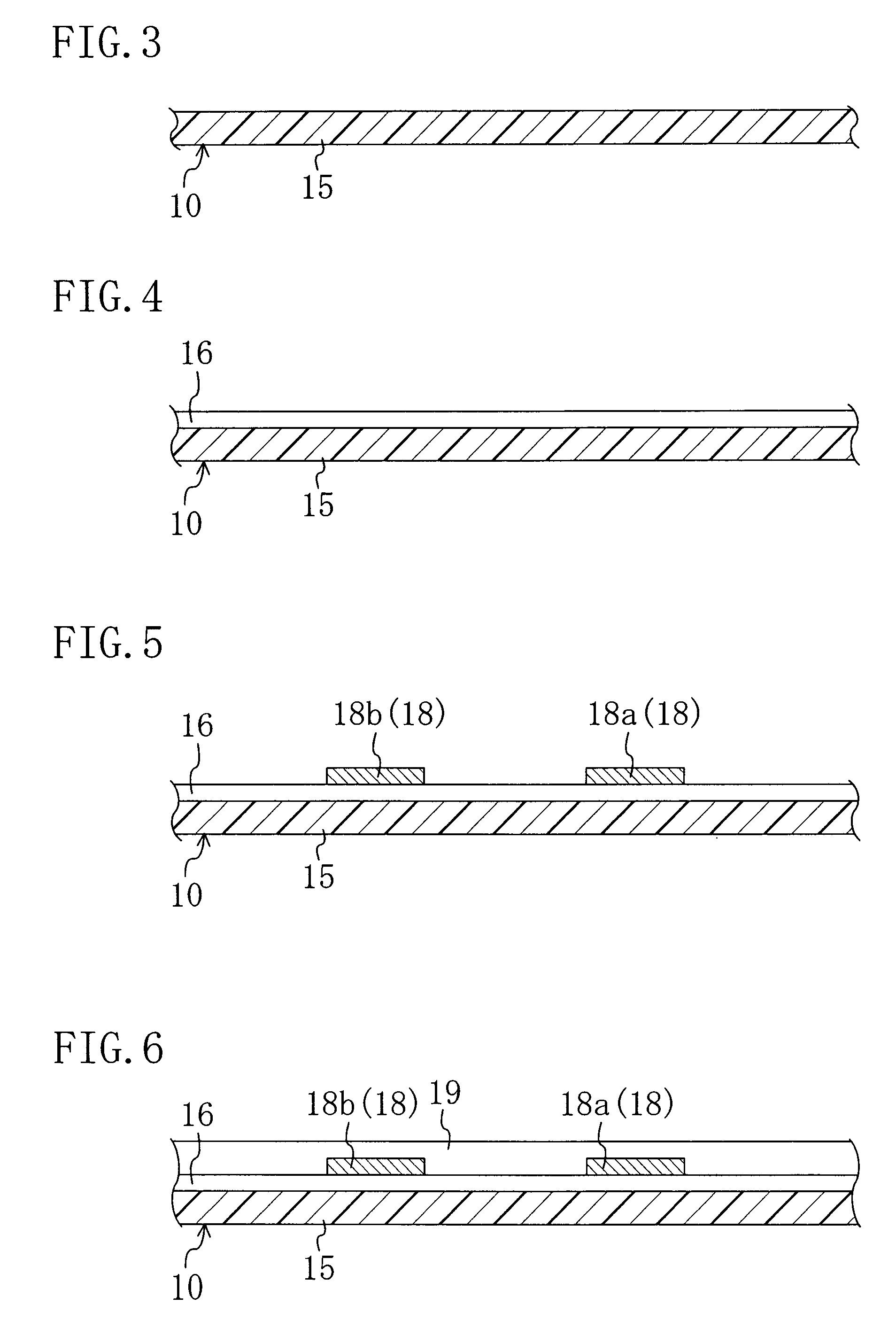
[0076]FIG. 1 to FIG. 8 show a first preferred embodiment of the present invention. FIG. 1 is a plan view illustrating the appearance of a liquid crystal display device 1 as a display device. FIG. 2 is a sectional view illustrating enlargement of an electrode connection structure 2. FIG. 3 to FIG. 8 are sectional views illustrating the steps of producing the electrode connection structure 2.

[0077]As shown in FIG. 1, the liquid crystal display device 1 includes a TFT substrate 10 as a first circuit component, a counter substrate 11 arranged to face the TFT substrate 10 and a liquid crystal layer (not shown) provided between the TFT substrate 10 and the counter substrate 11. An IC driver 12 as a second circuit component and an FPC (flexible printed circuit) 13 are implemented on the TFT substrate 10. The FPC 13 functions to supply signals to the IC driver 12 and the IC driver 12 functions to control and drive TFTs.

[0078]Though not shown, the TFT substrate 10 includes a plurality of TFT...

second preferred embodiment

[0105]FIG. 12 shows a second preferred embodiment of the present invention. In the following preferred embodiments, the same reference numerals are given to the same components as those shown in FIG. 1 to FIG. 8 to omit detailed explanation.

[0106]Different from the first preferred embodiment in which the strip-like portions of the barrier film 16 are left between the terminals 18 and the bumps 21, the barrier film 16 is not interposed between the terminals 18 and the bumps 21 in the present preferred embodiment.

[0107]The barrier film 16 is removed from not only the removed regions 26 but also regions below the terminals 18 and the insulating film 19. That is, the terminals 18 are formed directly on the surface of the plastic plate 15 of the TFT substrate 10.

[0108]For the production of the electrode connection structure of the present preferred embodiment, the barrier film 16 is uniformly formed on the plastic plate 15 as shown in FIG. 4, and then a portion of the barrier film 16 in ...

third preferred embodiment

[0111]FIG. 13 to FIG. 15 show a third preferred embodiment of the present invention. FIG. 13 is a sectional view schematically illustrating a liquid crystal display device 1 of the present preferred embodiment, FIG. 14 is a plan view schematically illustrating the appearance of the liquid crystal display device 1 of the present preferred embodiment and FIG. 15 is a plan view illustrating partial enlargement of a TFT substrate 10. FIG. 13 is depicted in a simple way and does not exactly correspond to FIG. 15.

[0112]In the liquid crystal display device 1 of the present preferred embodiment, a TFT substrate 10 as a first circuit component and a counter substrate 11 as a second circuit component include plastic plates 15 and 35, respectively. The plastic plate 15 of the TFT substrate 10 is provided with a barrier film 16 stacked on the surface thereof facing the counter substrate 11. The plastic plate 35 of the counter substrate 11 is provided with a barrier film 36 on the surface thereo...


PUM


Abstract

An electrode connection structure including a first circuit component including a resin plate, a barrier film stacked on a surface of the resin plate, a circuit section formed on the barrier film and a first electrode provided on the surface of the resin plate on which the barrier film is stacked, and a second circuit component arranged to face the first circuit component and having a second electrode facing the first electrode, wherein the first and second electrodes are electrically connected via pressure applied thereto in the directions approaching each other and a portion of the barrier film surrounding the first electrode is at least partially removed from the surface of the resin plate.

Description

BACKGROUND OF THE INVENTION[0001]1. Field of the Invention[0002]The present invention relates to a circuit component including a flexible plate on which a barrier film and electrodes are formed, an electrode connection structure for connection between the electrodes and a display device including the electrode connection structure.[0003]2. Description of the Related Art[0004]For display devices such as liquid crystal displays, organic EL displays and electrophoretic displays, an active matrix substrate has widely been used as a first circuit component prepared by forming a plurality of thin film transistors (hereinafter referred to as TFTs) on a glass plate.[0005]The TFTs are arranged in a matrix pattern. The active matrix substrate also carries thereon a plurality of source lines and gate lines arranged in a lattice pattern and connected to the TFTs. The source lines are arranged parallel to each other and the gate lines are arranged to be orthogonal to the source lines. The source...

Claims


Application Information

Patent Timeline
Patent Type & Authority Patents(United States)
IPC IPC(8): H05K1/00
CPCG02F1/13452H05K3/323H01L24/16H01L2924/07802H01L2224/293H01L2224/2929H05K2201/10674H05K2201/0989H05K2201/0179H05K3/388H05K3/386H01L24/83H01L2224/83192H01L2224/83851H01L2924/01004H01L2924/01078H01L2924/01079H05K3/3452H01L2924/3512H01L2924/00H01L2924/00014H01L2924/0665H01L2224/05572H01L2224/05573H01L2224/05599
Inventor AITA, TETSUYACHIKAMA, YOSHIMASA
Owner SHARP KK
Why Eureka
Try Eureka