Electrical element and electrical connector

a technology of electrical elements and connectors, applied in the field of electrical elements and electrical connectors, can solve the problems of affecting the quality of soldering, the terminals on the circuit board, and the volume after packaging is compact, and achieve the effect of reducing assembly errors and improving soldering quality

Inactive Publication Date: 2011-06-14
LOTES
View PDF2 Cites 6 Cited by
  • Summary
  • Abstract
  • Description
  • Claims
  • Application Information

AI Technical Summary

Benefits of technology

[0012]In order to achieve above object, the electrical element and the electrical connector of the present invention includes the conductive layer disposed on surface of the receiving hole. The conductive layer contacts with the soldering body so that the assembly between the soldering body and the terminal i...

Problems solved by technology

Yet the volume after packaging is getting compact.
Abundant terminals with high density make how to solder the terminals on the circuit board with good soldering quality become a dilemma.
However, all people skilled in this field learn that there are two errors that cause solder ball deformation in th...

Method used


Image

  • Electrical element and electrical connector
  • Electrical element and electrical connector
  • Electrical element and electrical connector

Examples


first embodiment

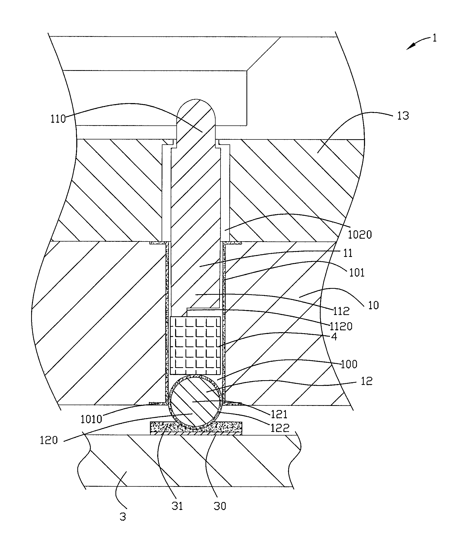
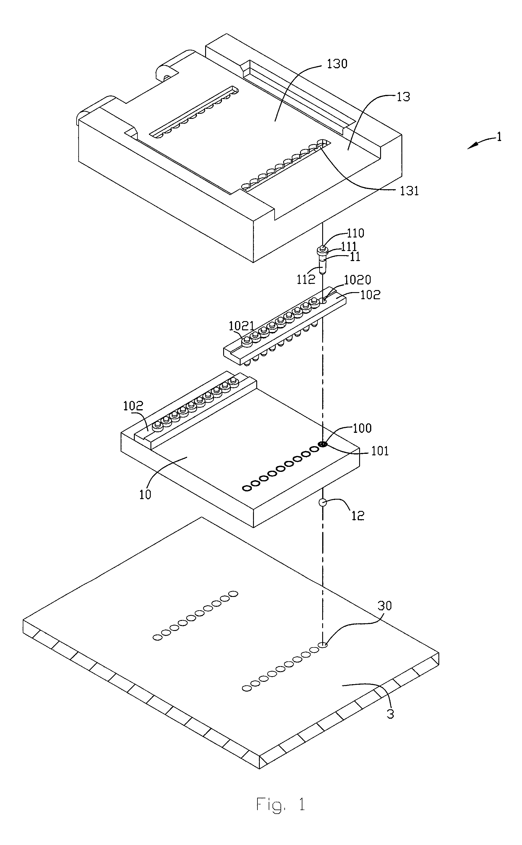
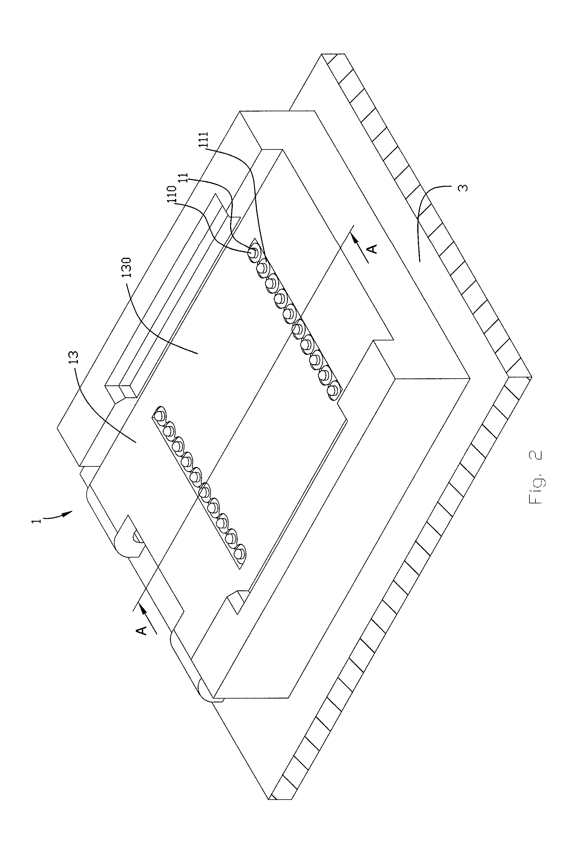
[0024]Refer from FIG. 1 to FIG. 4, an electrical element and an electrical connector according to the present invention is revealed. In this embodiment, the electrical element is an electrical connector 1 that electrically connects a chip module 2 to a circuit board 3, as shown in FIG. 4. The electrical connector 1 includes an insulating body 10, a cover 13 arranged over the insulating body 10, a plurality of conductive terminals 11 mounted in the insulating body 10, and a plurality of soldering bodies (the soldering bodies are solder balls 12 in this embodiment).

[0025]A plurality of receiving holes 100 are disposed on the insulating body 10, penetrating a top surface and a bottom surface thereof. A surface of each of the receiving hole 100 is coated with a conductive layer 101. A solder pad 1010 is arranged at the bottom surface of the insulating body 10, around the receiving hole 100. It will be mentioned later that a soldering part 120 of the solder ball 12 is also on this bottom...

second embodiment

[0034]Refer to FIG. 5 and FIG. 6, the electrical element and the electrical connector of the present invention is revealed. The difference between this embodiment is in that: the elastic body 102 has a flat top surface and there is a height difference between bottom surfaces on two sides of the press part 111. The left side bottom surface is lower than the right side bottom surface. After the electrical connector 1 being assembled and soldered, the chip module 2 is set above the cover 13 and is pressed downward. Then the conductive terminal 11 moves downward, the left side of the elastic body 102 serves as a support point (the elastic body 102 used as a stopper) and the press part 111 rotates to the right side of the elastic body 102 while the tail part 112 of the conductive terminal 11 rotates to the left side (the bottom surface of the press part 111 with lower height) and contacts with the conductive layer 101 slantingly so as to electrically connect with the conductive layer 101...

fourth embodiment

[0036]As shown in FIG. 9 and FIG. 10, the fourth embodiment is revealed. The difference between this embodiment and the above one is in that: a ball 5 is disposed between the rubber block 4 and the conductive terminal 11. Thereby when the conductive terminal 11 is pressed and contacted by the chip module 2, the conductive terminal 11 can slantingly contact with the conductive layer 101 more easily and reliably.

[0037]Moreover, the way of conducting by the connection between the soldering body and the conductive layer 101 and disposition of the conductive layer 101 as well as the soldering body in the receiving hole 100 in the present invention for replacement of the assembly of the terminal with the solder ball in techniques available now can also be applied to other electrical elements such as chips or circuit boards.

[0038]In summary, the electrical element and the electrical connector according to the present invention have following advantages:

[0039]1. The electrical element and t...


PUM


Abstract

An electrical element is revealed. At least one receiving hole disposes on an insulating body. A conductive layer disposes on surfaces of the receiving hole. At least one soldering body mounts in the receiving hole correspondingly and contacts with the conductive layer. Part of the soldering body exposes outside a surface of the insulating body to form a soldering part. The electrical element is further arranged with at least one conductive terminal mounted in the corresponding receiving hole movably and slantingly, the conductive terminal contacts with the conductive layer. Each conductive terminal includes a head part exposed outside the surface of the insulating body for being pressed and contacted. By electrical connection of the conductive layer, the assembly between the soldering body and the terminal is replaced and errors of the assembly between the soldering body and the terminal are eliminated. Therefore, the soldering quality is improved greatly.

Description

BACKGROUND OF THE INVENTION[0001]1. Field of the Invention[0002]The present invention relates to an electrical element and an electrical connector, especially to an electrical element and an electrical connector that are electrically connected to a circuit board.[0003]2. Description of Related Art[0004]Nowadays electrical connection points for inputting signals on chips increase along with the increasing of the processing speed and functions of integrated-circuit chips such as central processing unit (CPU). Yet the volume after packaging is getting compact.[0005]In order to catch up with the development of integrated-circuit (IC) chips such as CPU, the electrical connector that connects the IC chips with the circuit board includes more and more terminals with high density. Abundant terminals with high density make how to solder the terminals on the circuit board with good soldering quality become a dilemma. Presently, soldering is the most common way in this field. The electrical co...

Claims


Application Information

Patent Timeline
IPC IPC(8): H01R12/00H05K1/00
CPCH05K3/3436H05K3/301H05K2203/041H05K2201/10325H05K2201/10674H05K3/3484H05K3/3485Y02P70/50
Inventor JU, TED
Owner LOTES
Why Eureka
Try Eureka