Active biasing in metal oxide semiconductor (MOS) differential pairs

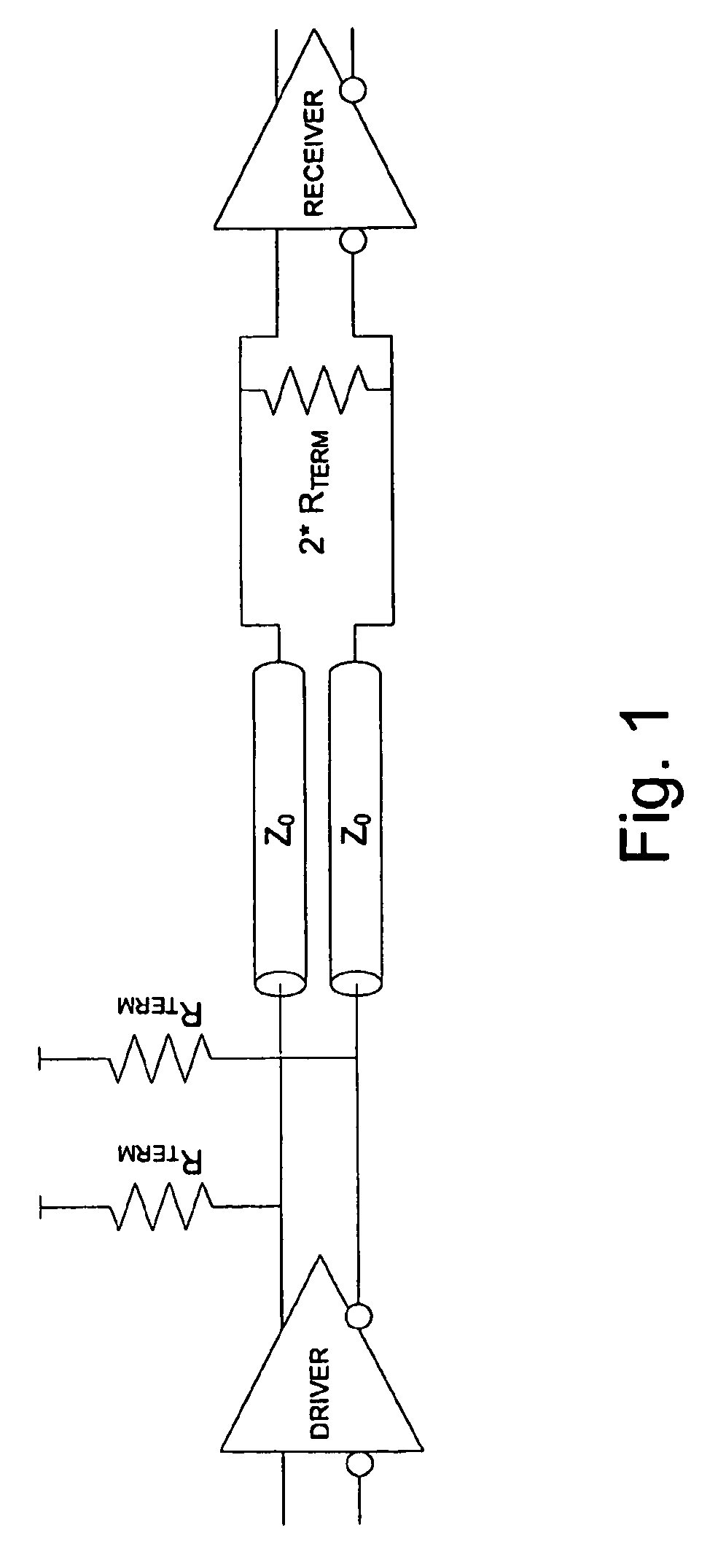
a technology of metal oxide semiconductor and differential pair, which is applied in the field of differential circuits using metaloxide semiconductor (mos) field effect transistors, can solve the problems of reducing the sensitivity of output swing to supply variation, affecting the integrity of received signals, and traditional approaches that are impractical

Inactive Publication Date: 2011-06-28
MICROSEMI STORAGE SOLUTIONS
View PDF6 Cites 18 Cited by
  • Summary
  • Abstract
  • Description
  • Claims
  • Application Information

AI Technical Summary

Problems solved by technology

When this is not the case, the impedance mismatches will typically create reflections that will affect the integrity of the received signal.
This reduces the sensitivity of the output swing to supply variations.
However, the use of deep-sub-micron technologies using low supply voltages, for example, on the order of 1V and less, renders this traditional approach impractical.
Accordingly, the objectives of relatively large output swings while keeping the output transistors in saturation, as required to achieve fast output transitions and good return loss, are difficult to achieve.
For large output swings in these technologies, or very large swings in higher voltage technologies, it is difficult to determine a static pre-driver high output voltage level that will guarantee the saturation of the differential pair transistors across process, voltage and temperature variations (PVT).

Method used


Image

  • Active biasing in metal oxide semiconductor (MOS) differential pairs
  • Active biasing in metal oxide semiconductor (MOS) differential pairs
  • Active biasing in metal oxide semiconductor (MOS) differential pairs

Examples


Embodiment Construction

[0046]Although particular embodiments are described herein, other embodiments, including embodiments that do not provide all of the benefits and features set forth herein, will be apparent to those of ordinary skill in the art.

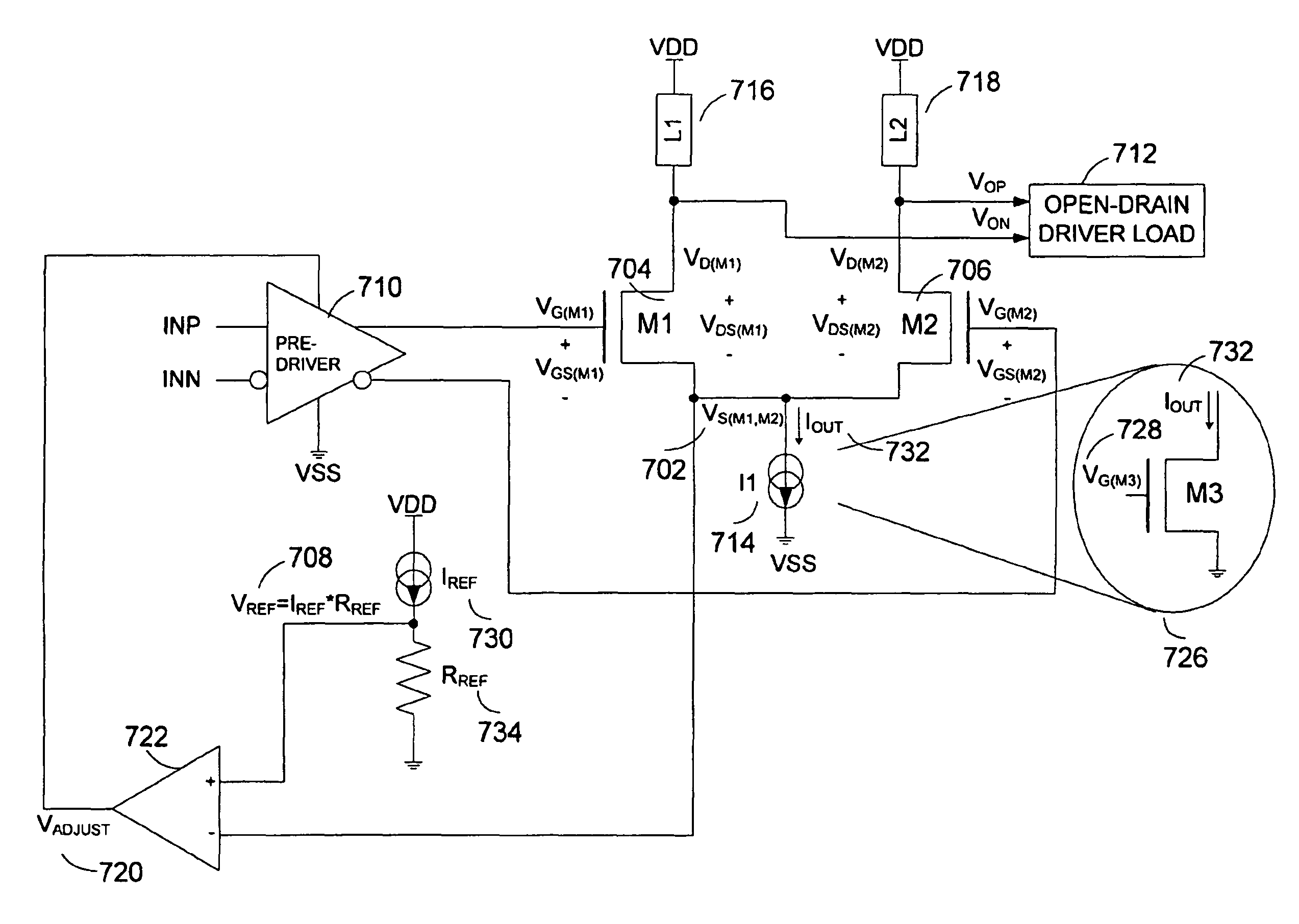
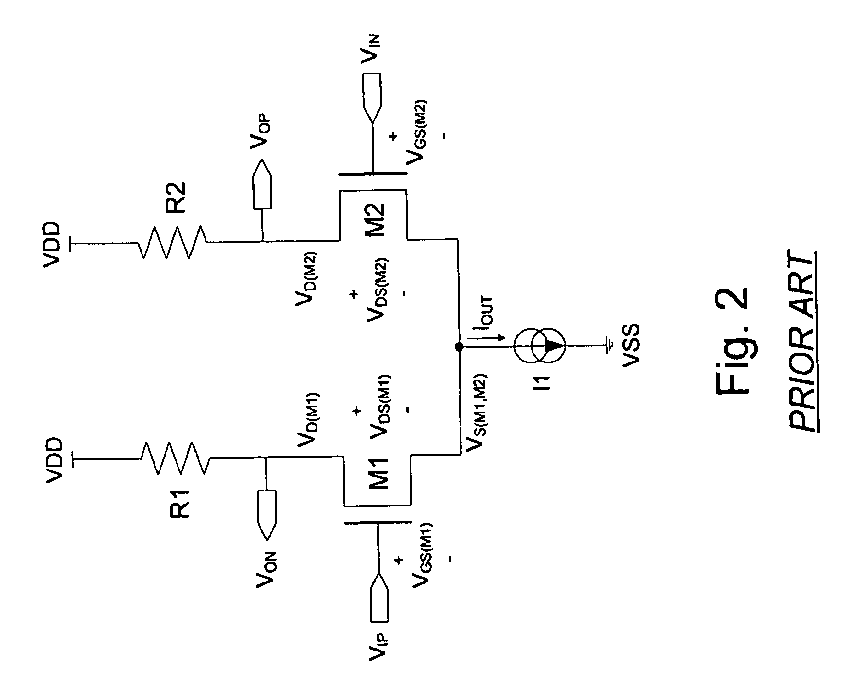
[0047]While generally illustrated in the context of differential circuits using N-type MOSFET (NMOS) transistors in the differential pairs, the skilled practitioner will appreciate that the principles and advantages described herein will also be applicable to differential circuits using P-type (PMOS) transistors in the differential pairs. In addition, the principles and advantages described herein can also be applied to differential drivers that use a combination of an NMOS and a PMOS differential pairs. Such structures are relatively common in low voltage differential signaling (LVDS) drivers. Examples of differential signaling protocols include XAUI, CEI-6, SAS, SATA, FiberChannel, and the like. For example, biasing circuits and corresponding drivers can be ...


PUM


Abstract

Apparatus and methods advantageously maintain transistors of open-drain differential pairs biased in the saturation region when “active,” rather in than the triode or linear region. The biasing techniques are effective over a broad range of process, voltage, and temperature (PVT) variations. By controlling a high voltage level used to drive the gate of a transistor of the differential pair, the biasing of the transistor in the saturation region is maintained. In one embodiment, the low voltage level used to cut off the transistor of the differential pair is also controlled. These techniques advantageously permit differential drivers to exhibit relatively large output swings, relatively high edge rates, relatively high return loss, and relatively good efficiency.

Description

CROSS-REFERENCE TO RELATED APPLICATIONS[0001]This application is a continuation application of U.S. application Ser. No. 11 / 128,953, filed May 12, 2005, now U.S. Pat. No. 7,471,107, issued Dec. 30, 2008, which claims the benefit under 35 U.S.C. §119(e) of U.S. Provisional Application No. 60 / 570,167, filed May 12, 2004, the disclosures of each of which are hereby incorporated by reference herein.BACKGROUND[0002]1. Field of the Invention[0003]The invention generally relates to differential circuits using metal-oxide semiconductor (MOS) field effect transistors (FETs). In particular, embodiments are applicable to the biasing of any MOS transistor differential pair configuration for which the gate voltage can be adjusted and biasing in the saturation region is desirable.[0004]2. Description of the Related Art[0005]Differential signaling is often used in high-speed data transmission systems in a variety of applications including in printed-circuit boards, cables and backplanes. When comp...

Claims


Application Information

Patent Timeline
Patent Type & Authority Patents(United States)
IPC IPC(8): H03K19/094
CPCH03K19/00384H03K19/018514H03K19/01707H03K17/145
Inventor FORTIN, GUILLAUMEROY, CHARLESGAGNON, MATHIEU
Owner MICROSEMI STORAGE SOLUTIONS
Why Eureka
Try Eureka