Top-gate thin-film transistors using nanoparticles and method of manufacturing the same

a technology of nanoparticles and transistors, applied in the direction of nanotechnology, electrical equipment, semiconductor devices, etc., can solve the problems of direct application physical and chemical stability, and inherent limitations of organic thin-film transistors, so as to facilitate the formation of nanoparticle films and low-voltage operation

Active Publication Date: 2011-07-05
KOREA UNIV IND & ACADEMIC CALLABORATION FOUND
View PDF12 Cites 1 Cited by
  • Summary
  • Abstract
  • Description
  • Claims
  • Application Information

AI Technical Summary

Benefits of technology

[0010]The present invention is conceived to solve the aforementioned problems in the prior art. An object of the present invention is to provide top-gate thin-film transistors with channels composed of nanoparticle films formed on flexible substrates and a method of manufacturing the same, in which hydrophilic buffer layers are deposited on the flexible substrates to facilitate formation of nanoparticle films, and sintered nanoparticles are used as channel layers and gate dielectric layers are formed on the nanoparticle films, thereby enabling low-voltage operation and low-temperature fabrication.

Problems solved by technology

However, such organic thin-film transistors have inherent limitations in view of mobility, physical and chemical stability and the like.
Further, there are difficulties in that the organic thin-film transistors are directly applied to processes studied so far for inorganic semiconductors.

Method used


Image

  • Top-gate thin-film transistors using nanoparticles and method of manufacturing the same
  • Top-gate thin-film transistors using nanoparticles and method of manufacturing the same
  • Top-gate thin-film transistors using nanoparticles and method of manufacturing the same

Examples


Embodiment Construction

[0034]Hereinafter, a preferred embodiment of a method of manufacturing a thin-film transistor using nanoparticles according to the present invention will be described in detail with reference to the accompanying drawings.

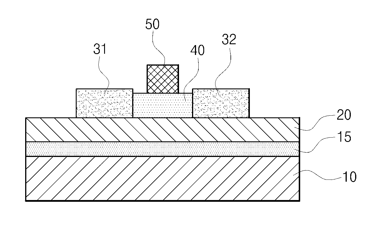
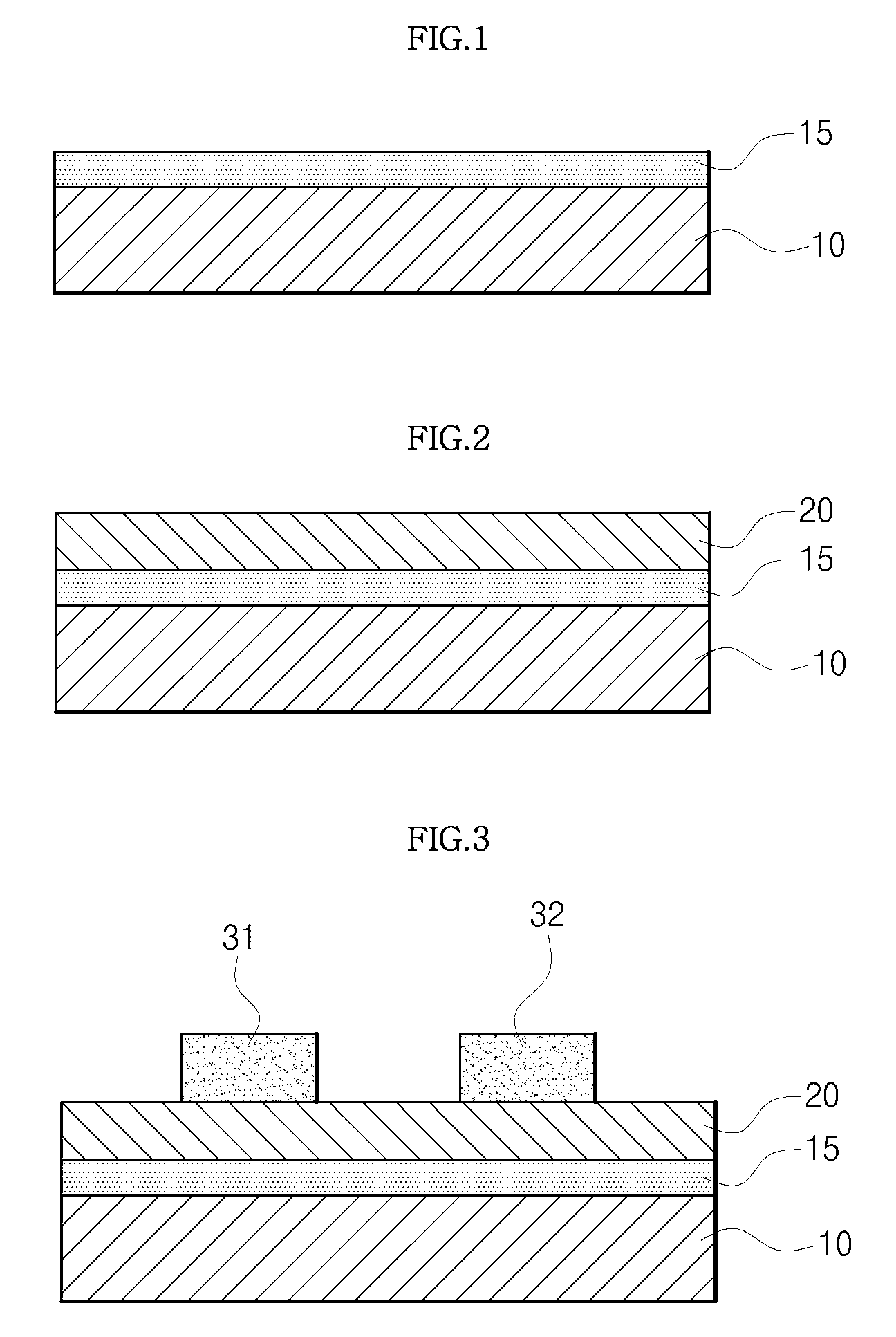
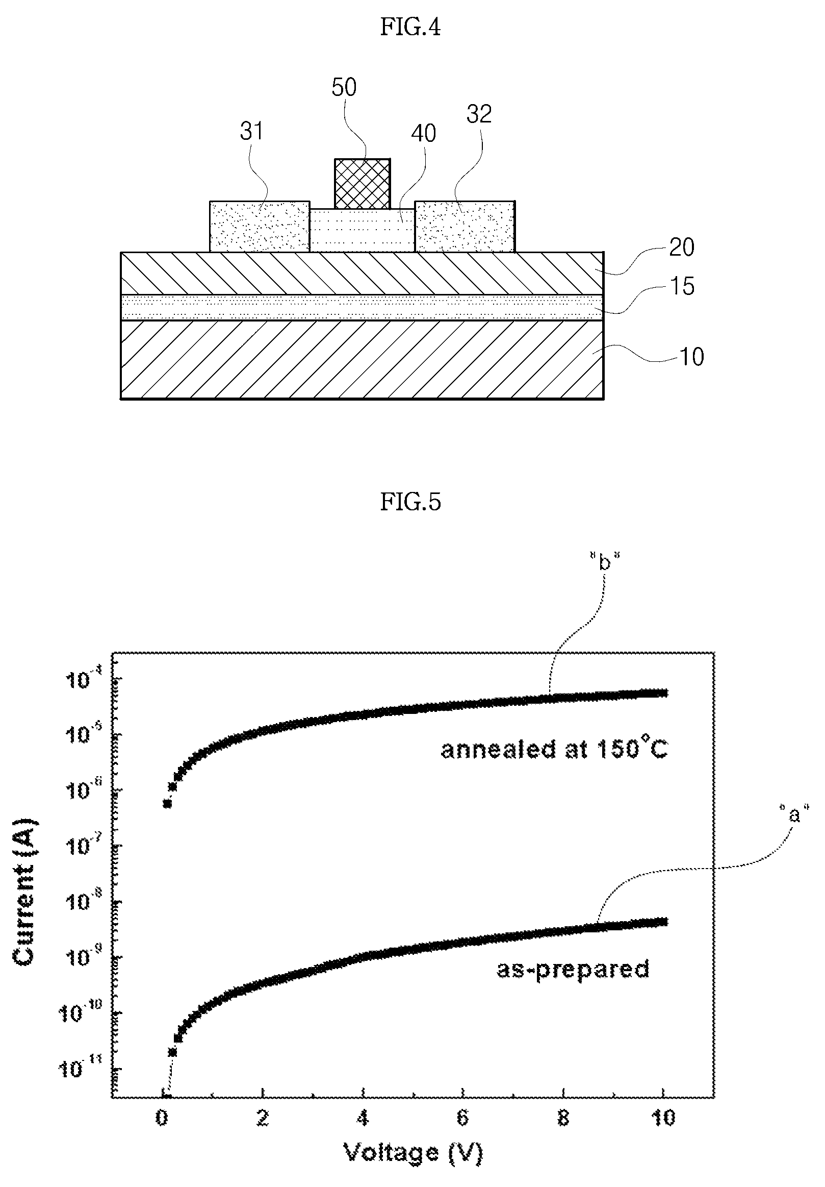
[0035]A method of manufacturing a thin-film transistor using nanoparticles according to the present invention basically comprises the steps of forming a nanoparticle film on a substrate and then sintering the nanoparticle film, forming source and drain electrodes on the nanoparticle film, forming a gate dielectric layer by depositing dielectric material on the nanoparticle film formed with the source and drain electrodes, and forming a top gate electrode on the gate dielectric layer.

[0036]The method of manufacturing thin-film transistors using nanoparticles according to the present invention may further comprise the step of depositing buffer layers between the substrate and the nanoparticle film using hydrophilic materials. At this time, the substrate may be any one...


PUM

PropertyMeasurementUnit
thicknessaaaaaaaaaa
temperatureaaaaaaaaaa

Abstract

The present invention relates to a method of manufacturing thin-film transistors using nanoparticles and thin film transistors manufactured by the method. A hydrophilic buffer layers are deposited on the substrates to facilitate formation of nanoparticle films. Sintered nanoparticles are used as an active layer and dielectric materials of high dielectric coefficient are also used as a gate dielectric layer to form a top gate electrode on the gate dielectric layer, thereby enabling low-voltage operation and low-temperature fabrication.

Description

BACKGROUND OF THE INVENTION[0001]1. Field of the Invention[0002]The present invention relates to a method of manufacturing thin-film transistors using nanoparticles and thin-film transistors manufactured by the method. More particularly, the present invention relates to top-gate thin-film transistors formed on flexible substrates using nanoparticles and a method of manufacturing the same, in which hydrophilic buffer layers are deposited on the substrates to facilitate formation of nanoparticle films, and sintered nanoparticles are used as channel layers of the thin-film transistors and dielectric materials of high dielectric constant are also used as gate layers to form top gate electrodes on the gate dielectric layers, thereby enabling low-voltage operation and low-temperature fabrication.[0003]2. Description of the Related Art[0004]In general, field-effect thin-film transistors currently used in flat panel display including a liquid crystal display (LCD) are manufactured by using ...

Claims


Application Information

Patent Timeline
Patent Type & Authority Patents(United States)
IPC IPC(8): H01L21/477
CPCB82Y10/00H01L29/0665H01L29/0673H01L29/78603H01L29/78681H01L29/7869H01L29/78696Y10S977/773Y10S977/936Y10S977/824Y10S977/892
Inventor KIM, SANGSIGCHO, KYOUNG-AHKIM, DONG-WONJANG, JAE-WON
Owner KOREA UNIV IND & ACADEMIC CALLABORATION FOUND
Why Eureka
Try Eureka