Thin film integrated circuit device, IC label, container comprising the thin film integrated circuit, manufacturing method of the thin film integrated circuit device, manufacturing method of the container, and management method of product having the container

a technology of integrated circuits and integrated circuits, which is applied in the direction of solid-state devices, transistors, instruments, etc., can solve the problems of inefficient manual reading of products, limited amount of information which can be provided, and time-consuming manual reading

Inactive Publication Date: 2011-07-05
SEMICON ENERGY LAB CO LTD
View PDF110 Cites 42 Cited by
  • Summary
  • Abstract
  • Description
  • Claims
  • Application Information

AI Technical Summary

Problems solved by technology

Further, when bar codes are used, it requires time to manually read each product.
When the information management is performed by using bar codes according with such increase in information, the amount of information which can be provided is limited.
It is inefficient spending time for reading manually, in addition to the lack of information.
Further, reading errors due to the manual operation of bar code reading can not be

Method used


Image

  • Thin film integrated circuit device, IC label, container comprising the thin film integrated circuit, manufacturing method of the thin film integrated circuit device, manufacturing method of the container, and management method of product having the container
  • Thin film integrated circuit device, IC label, container comprising the thin film integrated circuit, manufacturing method of the thin film integrated circuit device, manufacturing method of the container, and management method of product having the container
  • Thin film integrated circuit device, IC label, container comprising the thin film integrated circuit, manufacturing method of the thin film integrated circuit device, manufacturing method of the container, and management method of product having the container

Examples


embodiment mode 1

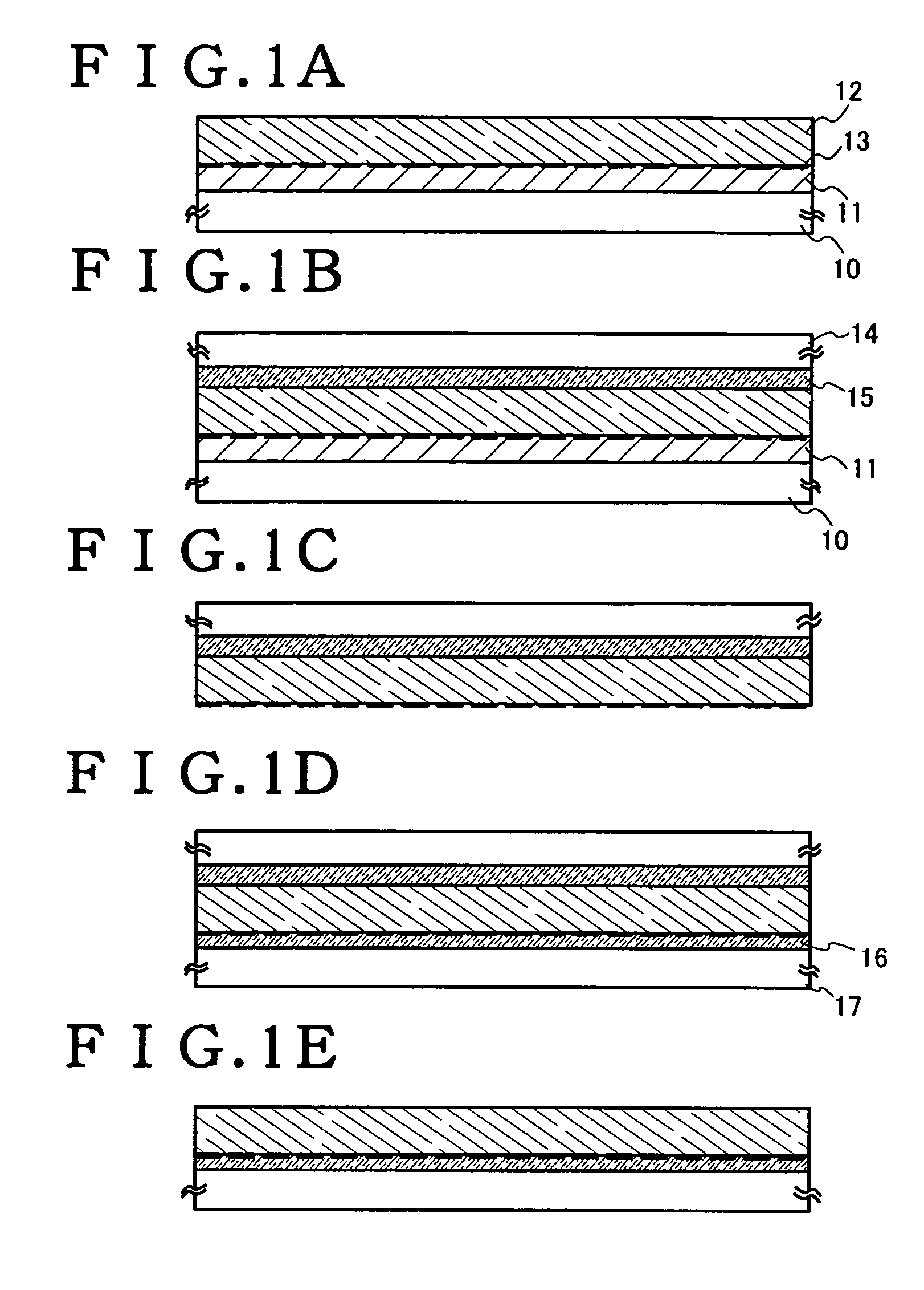
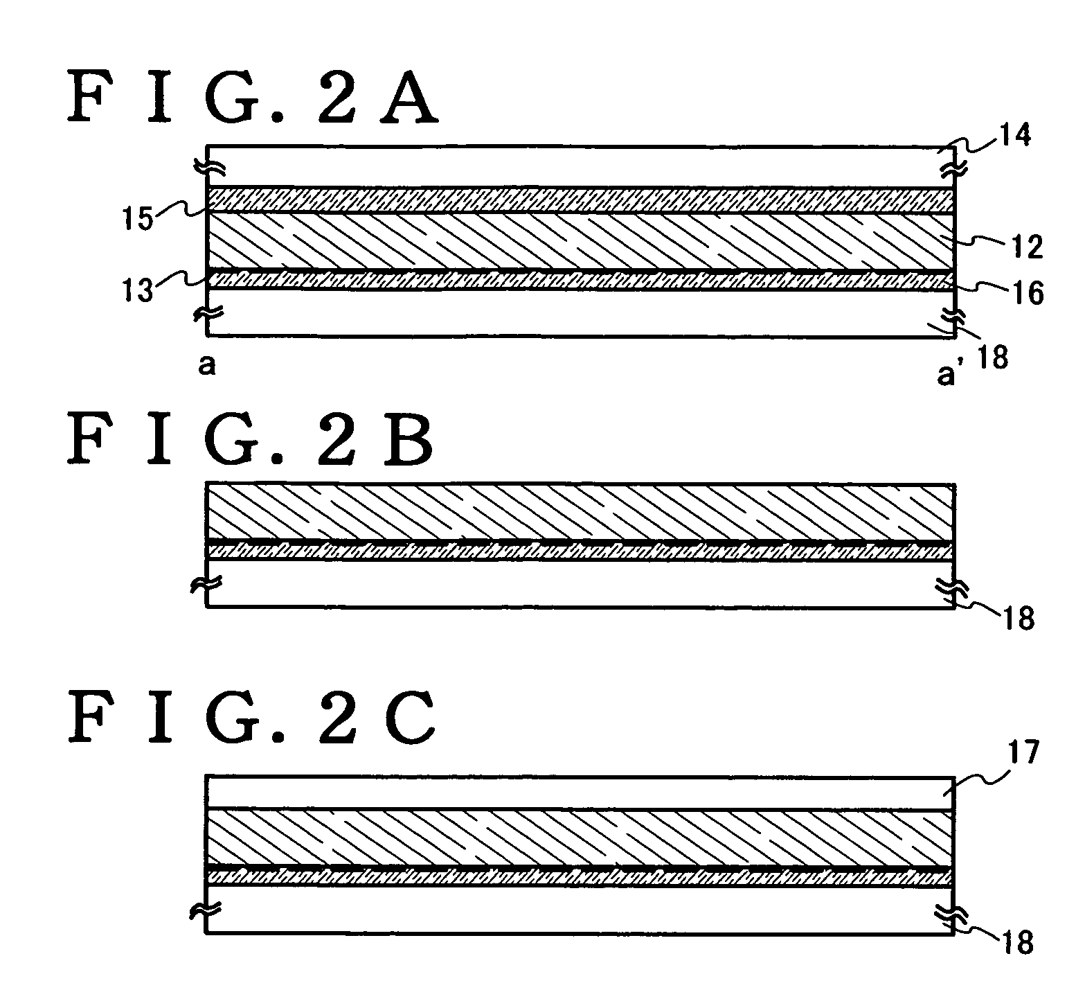
[0031]In this embodiment mode, a manufacturing method of a thin film integrated circuit according to the present invention using techniques of delamination and transfer will be described.

[0032]First, a metal film 11 is formed over a first substrate 10 as shown in FIG. 1A. Note that any substrate that has rigidity for withstanding the following lamination process, for example, a glass substrate, a quartz substrate, a ceramic substrate, a silicon substrate, a metal substrate, or a stainless substrate, can be used for the first substrate. A single layer or a laminate of an element selected from the group consisting of W, Ti, Ta, Mo, Nd, Ni, Co, Zr, Zn, Ru, Rh, Pd, Os, and Ir; an alloy material or a compound material which mainly includes the element can be used for the metal film. For example, the metal film can be formed by sputtering using a metal target. Note that, the film thickness of the metal film may be 10 nm to 200 nm, preferably be 50 nm to 75 nm.

[0033]Instead of the metal fi...

embodiment mode 2

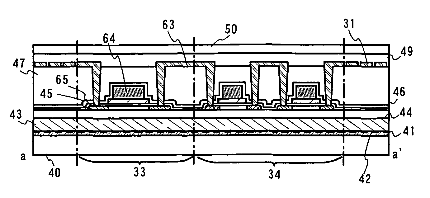
[0061]In this embodiment mode, the structure of a thin film integrate circuit and the principle of a contactless thin film integrated circuit will be explained. The contactless thin film integrated circuit is applied to an IC label that can be read without contact.

[0062]First, the principle of the contactless thin film integrated circuit is shown in a block diagram in FIG. 5. A contactless thin film integrated circuit 50 has a CPU 51, a memory 52, an I / O port 53, and a coprocessor 54 and exchanges data via a path 55. Further, the IC has an RFID (wireless) interface 56 and a contactless interface 57. A reader / writer 60 that serves as a reading means has a contactless interface 61 and an interface circuit 62. The IC is held to the reader / writer, and transmission of information or information exchange is performed between the contactless interfaces over radio waves. The transmission of information or information exchange with a host computer is performed by the interface circuit of the...

embodiment mode 3

[0088]In this embodiment mode, a method for reading information as for a product that is equipped with an IC label will be explained. In specific, the case where the IC label is a contactless type will be explained.

[0089]A product equipped with an IC label 72 is held to a sensing area 71 of a reader / writer body 70 shown in FIG. 7A. In addition to a material, the place of production, a test result of each production (manufacturing) process, a record of distribution process, and the like; information on a product such as a description of the product are displayed in a display area. The display area is not necessarily provided in the reader / writer, and may be formed separately. Such a reader / writer may be provided on a display rack.

[0090]As shown in FIG. 7B, for example, a personal digital assistant such as a cellular phone 80 is provided with a reading function therein; a product including an IC label 82 is held to a sensing area 81 that is installed in the main body. Then, informatio...


PUM


Abstract

The present invention provides an ultrathin thin film integrated circuit and a thin film integrated circuit device including the thin film integrated circuit device. Accordingly, the design of a product is not spoilt while an integrated circuit formed from a silicon wafer, which is thick and produces irregularities on the surface of the product container. The thin film integrated circuit according to the present invention includes a semiconductor film as an active region (for example a channel region in a thin film transistor), unlike an integrated circuit formed from a conventional silicon wafer. The thin film integrated circuit according to the present invention is thin enough that the design is not spoilt even when a product such as a card or a container is equipped with the thin film integrated circuit.

Description

BACKGROUND OF THE INVENTION[0001]1. Field of the Invention[0002]The present invention relates to a thin film integrated circuit device equipped with a thin film integrated circuit that is flexible and paper-thin that has a memory and a microprocessor (central processing unit (CPU)); an integrated circuit (IC) label using a thin film integrated circuit device for a label; a product container including the thin film integrated circuit; and manufacturing methods thereof. The present invention further relates to management methods of the products above.[0003]2. Description of the Related Art[0004]In late years, the number of cards that a person owns is increasing. Every kind of information is recorded in cards and is renewed as necessary. The amount of recorded information is progressively increasing.[0005]Such increase in the amount of information is essential in various fields. For example, in the food industry and manufacturing industry, as improvements in the product safety and the ...

Claims


Application Information

Patent Timeline
IPC IPC(8): H01L27/12H01L29/66G06K19/077H01L21/77H01L21/84H01L29/786
CPCG06K19/07749H01L29/78603H01L27/1214H01L27/12H01L27/1266H01L27/1218H04B1/38
Inventor ARAI, YASUYUKIISHIKAWA, AKIRATAKAYAMA, TORUMARUYAMA, JUNYAGOTO, YUUGOOHNO, YUMIKOTACHIMURA, YUKO
Owner SEMICON ENERGY LAB CO LTD
Why Eureka
Try Eureka