Conductive film and method of producing thereof

a conductive film and film technology, applied in the direction of conductive layers on insulating supports, photosensitive materials, instruments, etc., can solve the problems of erroneous operations and troubles, troublesome health of operators of such equipment, and increase in electromagnetic interference (emi) , to achieve the effect of low cost and high conductivity

Inactive Publication Date: 2011-07-26
FUJIFILM CORP
View PDF23 Cites 46 Cited by
  • Summary
  • Abstract
  • Description
  • Claims
  • Application Information

AI Technical Summary

Benefits of technology

[0016]In light of such a situation, the present invention has been made. An object of the present invention is to provide a method for producing a conductive film having a high conductivity at low cost.

Problems solved by technology

With the recent increase in the utilization of various electric facilities and electronic applied equipment, electromagnetic interference (EMI) has been increasing significantly.
Such EMI not only induces erroneous operations and troubles on electronic / electric equipment but also is pointed out to cause troubles on the health of operators of such equipment.
However, the silver mesh yielded by this method is large in line width since the mesh is formed by printing; thus, problems such as lowering of transmittance can arise.
Moreover, a surface resistance value is high and an electromagnetic wave shielding ability is small.
However, this producing method has a problem that only a mesh having a large surface resistance value of 10 Ω / sq (low electromagnetic wave shielding ability) is obtained.
Additionally, a haze is as large as ten plus several percentage or more, so as to result in a problem that the display images become obscure.
However, it has a disadvantage that the mesh has to be manufactured through a number of production steps.
Therefore, the method had a problem to cause a decrease in the image contrast of the display equipment.
However, this conductive level is insufficient for PDPs.
Thus, even if the silver salt diffusion transferring method was used as it was, it was impossible to obtain a translucent, electromagnetic wave shielding material excellent in optical transmittance and conductivity, which was suitable for shielding electromagnetic waves emitted from an image-displaying face of an electronic display instrument.
As explained above, the prior electromagnetic shield materials and the producing methods therefor have been associated with drawbacks.
Further, since such electromagnetic shield materials were very expensive, a reduction in the production cost has been strongly desired.
However, an increase in the aperture rate (a proportion of an area without the fine lines constituting the mesh) in the whole area for improving the optical transmittance reduces the conductivity to deteriorate the electromagnetic shielding effect.

Method used


Image

  • Conductive film and method of producing thereof
  • Conductive film and method of producing thereof
  • Conductive film and method of producing thereof

Examples


example 1-1

(Preparation of Emulsion A)

[0296]To the following solution 1, while the temperature and the pH of which were kept at 38° C. and 4.5, respectively, the following solutions 2 and 3 (amounts corresponding to 90% of the respective solution amounts) were added simultaneously over a period of 20 minutes with being stirred. In this way, nucleus particles 0.16 μm in size were formed. Subsequently, the following solutions 4 and 5 were added thereto over a period of 8 minutes, and the rests of the solutions 2 and 3 (amounts corresponding to 10% of the respective solution amounts) were further added thereto over a period of 2 minutes so as to cause the particles to grow up to 0.21 μm in size. Furthermore, 0.15 g of potassium iodide was added thereto, and the resultant was aged for 5 minutes to end the formation of the particles.

Solution 1:

[0297]

Water750mlGelatin (phthalation-treated gelatin)20gSodium chloride3g1,3-Dimethylimidazolidine-2-thione20mgSodium benzenethiosulfonate10mgCitric acid0.7g...

example 1-2

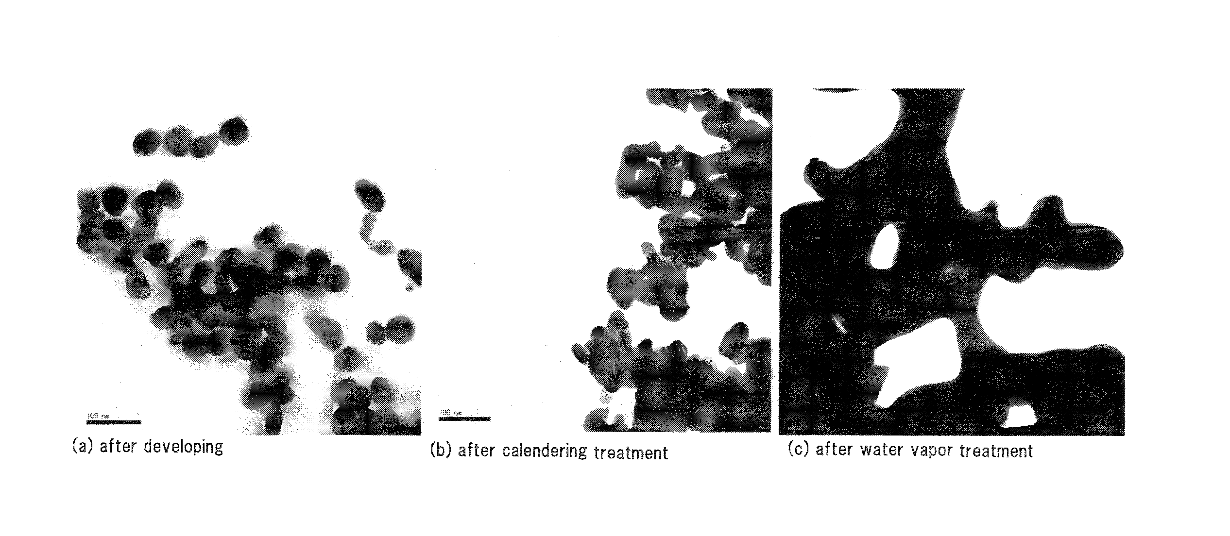
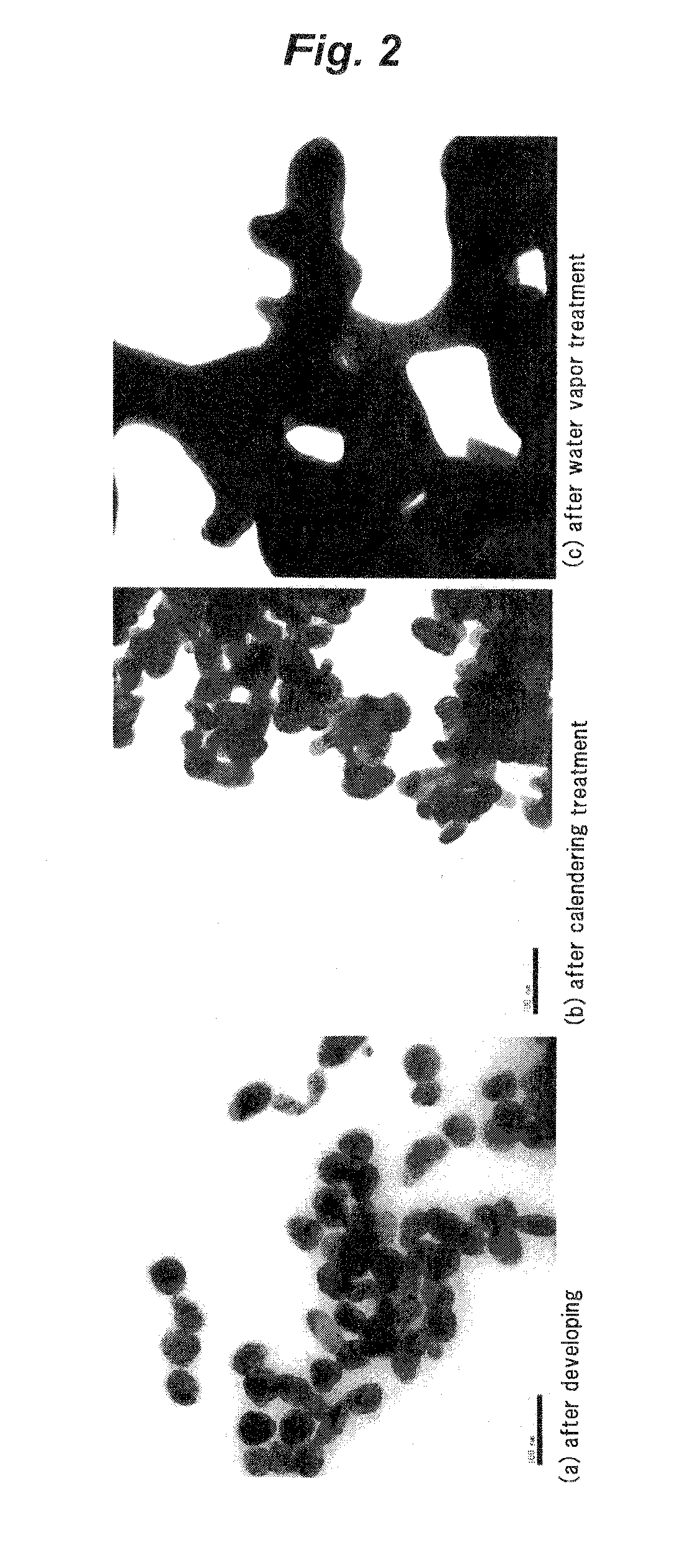
[0318]Samples prepared and subjected to exposing and developing treatments in the same way as in Example 1-1 were each subjected to a calendering treatment and a vapor contacting treatment. The calendering treatment was conducted in the same way as in Example 1-1 except that the load was changed.

[0319]Out of the resultant samples, one subjected to no calendering treatment and brought into contact with vapor for 30 seconds was named sample 1201; ones subjected to the calendering treatment with loads of 1,960 N / cm (200 kgf / cm), 2,940 N / cm (300 kgf / cm), 3,920 N / cm (400 kgf / cm), 5,880 N / cm (600 kgf / cm) and 6,860 N / cm (700 kgf / cm), respectively, and then brought into contact with vapor for 30 seconds were named sample 1202 to 1206, respectively; and ones brought into contact with vapor for 30 seconds and then subjected to the calendering treatment with loads of 1,960 N / cm (200 kgf / cm), 2,940 N / cm (300 kgf / cm), 3,920 N / cm (400 kgf / cm), 5,880 N / cm (600 kgf / cm) and 6,860 N / cm (700 kgf / cm), ...

example 1-3

[0326]Samples prepared and subjected to exposing and developing treatments and calendering treatment in the same way as in Example 1-1 were each subjected to a vapor contacting treatment as follows: the vapor contacting treatment was conducted in the same way as in Example 1-1 except that the vapor temperature was changed.

[0327]Out of the resultant samples, one treated at 80° C. was named sample 1301, one treated at 90° C. was named sample 1302, one treated at 100° C. was named sample 1303, one treated at 110° C. was named sample 1304, one treated at 120° C. was named sample 1305, and one treated at 130° C. was named sample 1306.

[0328]With respect to each of the samples, the surface resistance thereof was measured in the same way as in Example 1-1 before and after the vapor contacting treatment. The width of lines of the lattice pattern was measured in the same way as in Example 1-2. The results are shown in Table 3 below.

[0329]

TABLE 3SurfaceSurfaceresistanceresistanceTemperaturebef...


PUM

PropertyMeasurementUnit
temperatureaaaaaaaaaa
transparencyaaaaaaaaaa
visible light transmittanceaaaaaaaaaa

Abstract

A method for producing a conductive film, having the steps: forming, on a support, a conductive metal portion containing a conductive material and a binder; bringing the conductive metal portion into contact with vapor or a hot water; and immersing the conductive metal portion into hot water having a temperature of 40° C. or higher.

Description

TECHNICAL FIELD[0001]The present invention relates to a method for producing a conductive film having an improved conductivity, in particular, a translucent conductive film. More specifically, the present invention relates to a method for producing a conductive film by forming, on a support, a conductive metal portion containing a conductive material and a binder, and then treating the resultant metal portion with hot water or vapor.BACKGROUND ART[0002]With the recent increase in the utilization of various electric facilities and electronic applied equipment, electromagnetic interference (EMI) has been increasing significantly. Such EMI not only induces erroneous operations and troubles on electronic / electric equipment but also is pointed out to cause troubles on the health of operators of such equipment. It is therefore required, in such electronic / electric equipment, to restrict an intensity of an electromagnetic emission within a standard or regulated range.[0003]As a countermeas...

Claims


Application Information

Patent Timeline
Patent Type & Authority Patents(United States)
IPC IPC(8): G03F7/00G03F7/26G03F7/06
CPCH05K3/106H05K3/22H05K9/0096H05K1/095Y10T29/49155H05K2203/0786H05K2203/088H01B13/00H01B5/14H05K9/00G03C1/00
Inventor TOKUNAGA, TSUKASA
Owner FUJIFILM CORP
Why Eureka
Try Eureka