Trench-type semiconductor device structure

a semiconductor device and structure technology, applied in semiconductor devices, capacitors, electrical devices, etc., can solve the problems of affecting the performance of the device, the capacity of the device may not be increased, and the process of making the mosfet encounters many difficulties and problems

Active Publication Date: 2011-07-26
NAN YA TECH
View PDF17 Cites 1 Cited by
  • Summary
  • Abstract
  • Description
  • Claims
  • Application Information

AI Technical Summary

Benefits of technology

[0005]One aspect of the present invention is to provide a trench-type semiconductor device structure, which has a doped channel layer, so that the accumulated charge can be transferred to the substrate through the doped channel layer to avoid floating body effect.
[0006]Another aspect of the present invention is to provide a trench-type semiconductor device structure, wherein the channel width of the vertical transistor can be accurately controlled by using an epitaxial growth method.
[0007]Further aspect of the present invention is to provide a trench-type semiconductor device structure, wherein the process of forming a single-sided buried strap structure is performed after the process of forming the trench isolation layer to avoid excessive diffusions of the doped ions.
[0008]Still another aspect of the present invention is to provide a trench-type semiconductor device structure, wherein a reversed U-shaped gate dielectric layer slightly covers an epitaxial layer, so that the electric current passing through the epitaxial layer can be increased (i.e. the depletion region is increased).
[0009]Another aspect of the present invention is to provide a trench-type semiconductor device structure, wherein the process of forming a vertical transistor is performed after the process of forming a trench isolation layer, so that the damage of the gate dielectric layer can be avoided and the reliability of the device can be enhanced.

Problems solved by technology

However, as the device is scaled down to nano-level, the processes of making the MOSFET encounter many difficulties and problems.
If the problems caused and the size reduce of the device are not overcome, the capacity of the device may not be increased and / or the performance of the device will be negatively affected.

Method used


Image

  • Trench-type semiconductor device structure
  • Trench-type semiconductor device structure
  • Trench-type semiconductor device structure

Examples


Embodiment Construction

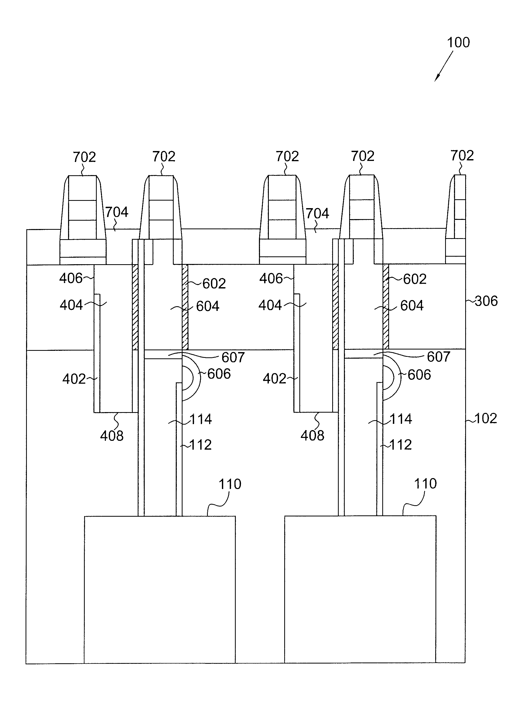
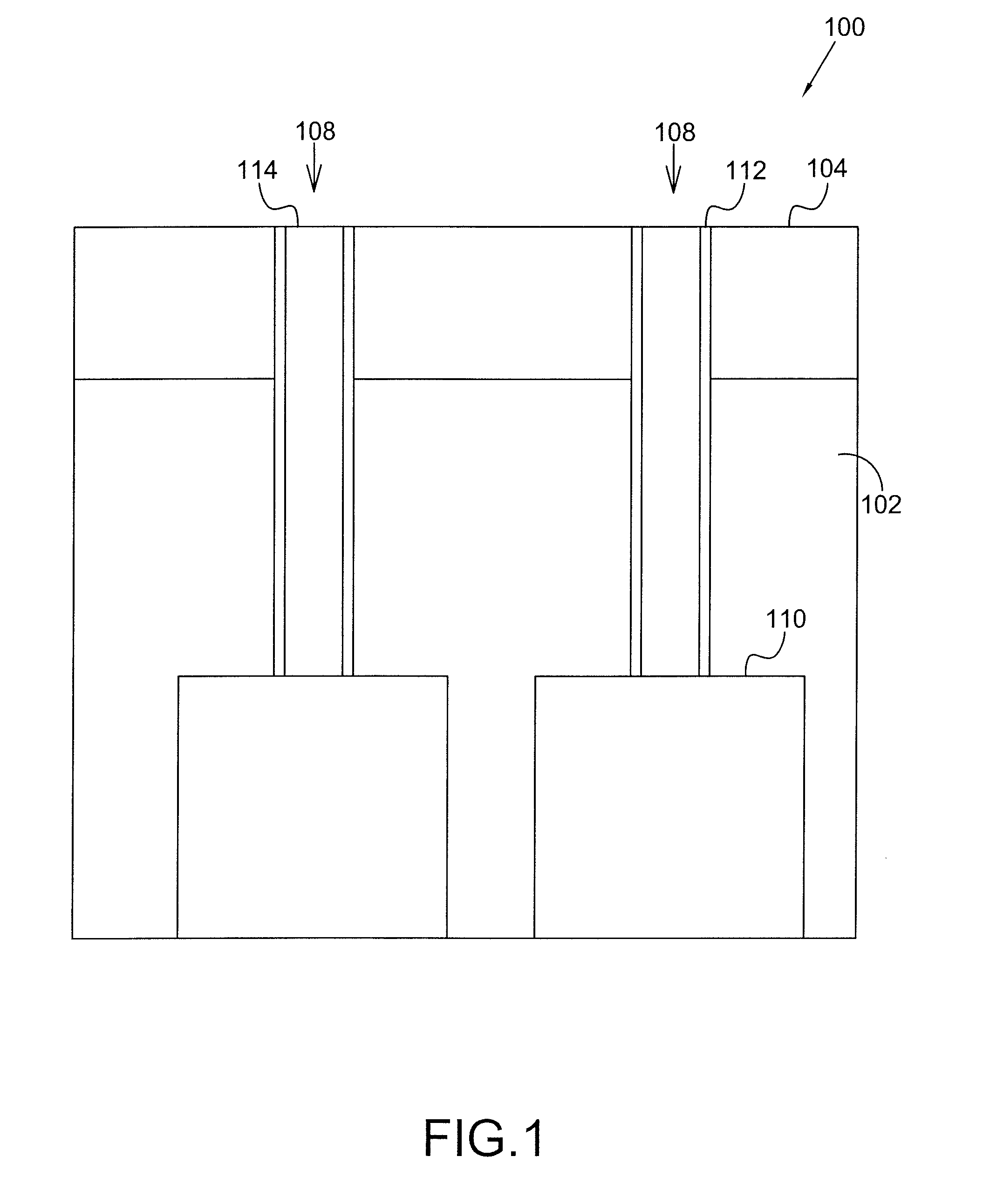
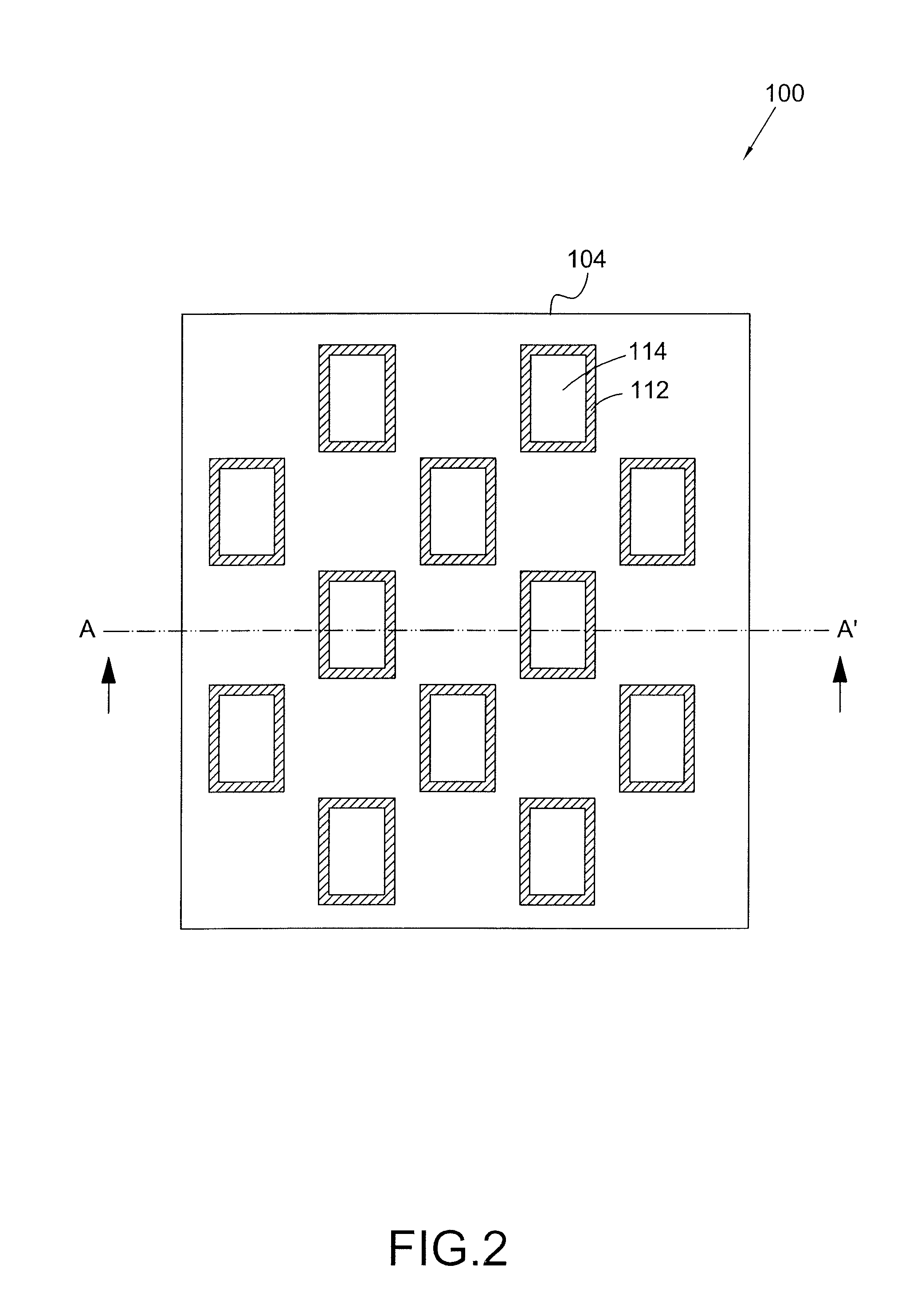
[0017]The present invention provides a trench-type semiconductor device structure and a method of forming the same in detail. Referring to FIG. 1 and FIG. 2, the semiconductor substrate 100 is provided, and then a trench 108 is formed in the semiconductor substrate 100. The semiconductor substrate 100 includes a silicon base layer 102 and a pad nitride layer 104 having a thickness of, for example, about 1350 Å. In one embodiment, the material of the silicon base layer 102 can be silicon (Si) or other similar semiconductor materials. The trench 108 has an upper portion and a lower portion. The lower portion of the trench 108 has a trench capacitor 110 formed therein, and the upper portion of the trench 108 has a collar dielectric layer 112 formed on an inner surface of the trench 108 and a conductive layer 114 filled in the trench 108. The conductive layer 114 can be, for example, a polysilicon layer or other conductive material layers. It should be noted that the formation of the tr...


PUM


Abstract

A trench-type semiconductor device structure is disclosed. The structure includes a semiconductor substrate, a gate dielectric layer and a substrate channel structure. The semiconductor substrate includes a trench having an upper portion and a lower portion. The upper portion includes a conductive layer formed therein. The lower portion includes a trench capacitor formed therein. The gate dielectric layer is located between the semiconductor substrate and the conductive layer. The substrate channel structure with openings, adjacent to the trench, is electrically connected to the semiconductor substrate via the openings.

Description

CROSS REFERENCE TO RELATED APPLICATIONS[0001]This application claims the right of priority based on Taiwan Patent Application No. 097100111 entitled “TRENCH-TYPE SEMICONDUCTOR DEVICE STRUCTURE,” filed on Jan. 2, 2008, which is incorporated herein by reference and assigned to the assignee herein.FIELD OF THE INVENTION[0002]This invention relates to a trench-type semiconductor device structure, and more particularly, to a trench-type semiconductor device by using the channel shielding to avoid floating body effect.BACKGROUND OF THE INVENTION[0003]As the manufacturing processes of the semiconductor devices are continuously improved, the feature size of the semiconductor device continually reduces to increase the quantity of the devices per area and to improve the capacity and the performance of the devices. For example, a traditional planar metal-oxide-semiconductor field-effect transistor (MOSFET) has been replaced by a trench-type semiconductor device to increase the quantity of the ...

Claims


Application Information

Patent Timeline
Patent Type & Authority Patents(United States)
IPC IPC(8): H01L27/108
CPCH01L27/10841H01L27/10864H01L27/10867H01L28/55H10B12/395H10B12/0383H10B12/0385
Inventor LIN, SHIAN-JYHCHANG, MING-CHENGSHIH, NENG TAILIAO, HUNG-CHANG
Owner NAN YA TECH
Why Eureka
Try Eureka