
Method of reducing wire bond profile height in integrated circuits mounted to circuit boards

a technology of integrated circuits and profile heights, which is applied in the direction of basic electric elements, solid-state devices, manufacturing tools, etc., can solve the problems of encapsulant bead hiccup, encapsulant volume and placement on the die is not very accurate, and the bead of encapsulant is not straigh

Inactive Publication Date: 2011-08-02
SILVERBROOK RES PTY LTD +1
View PDF18 Cites 6 Cited by
  • Summary
  • Abstract
  • Description
  • Claims
  • Application Information

AI Technical Summary

Benefits of technology

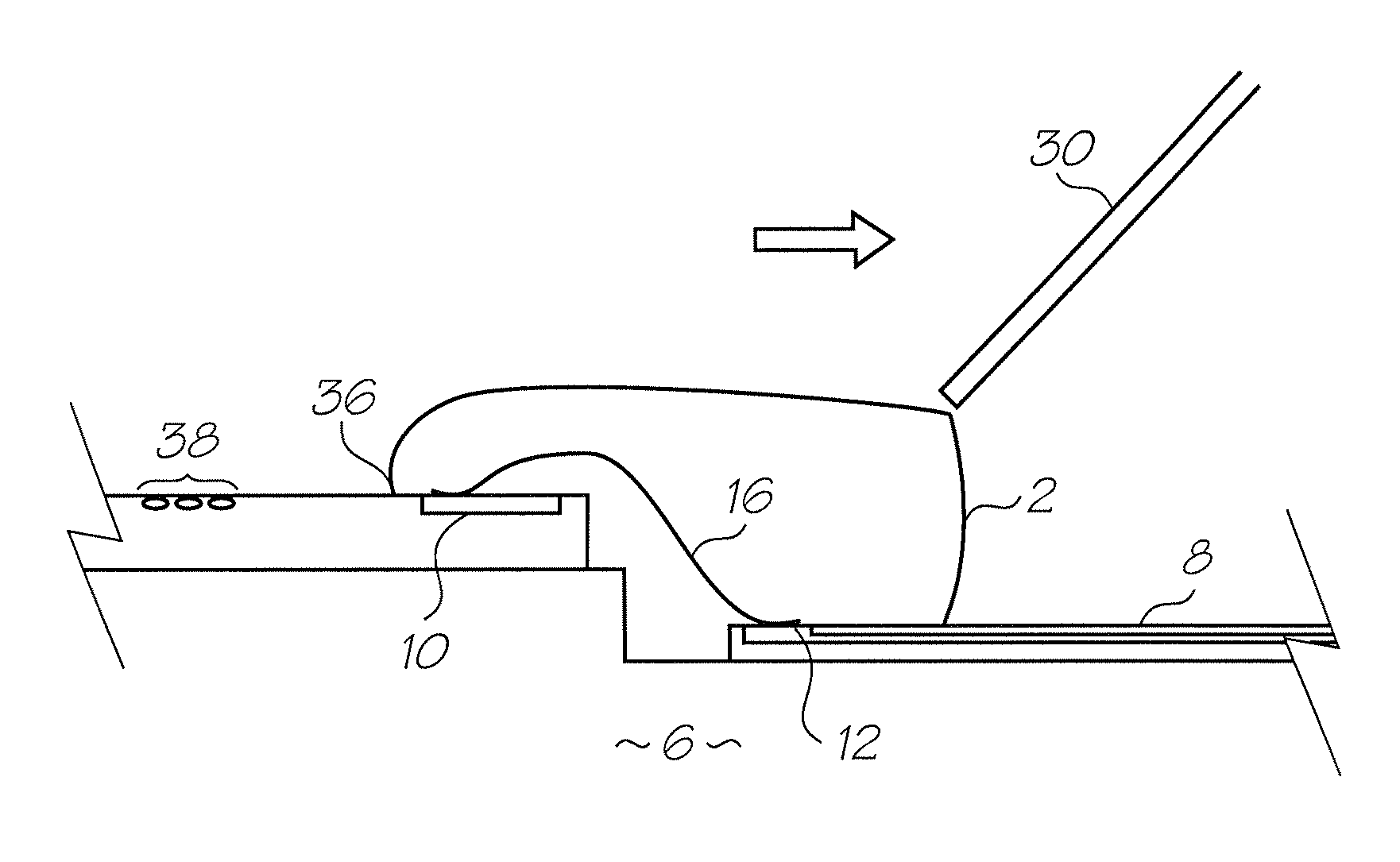
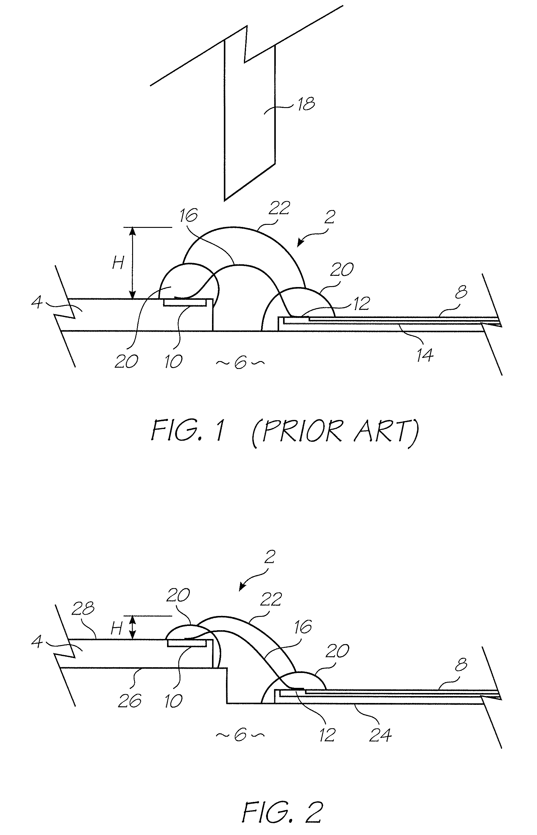
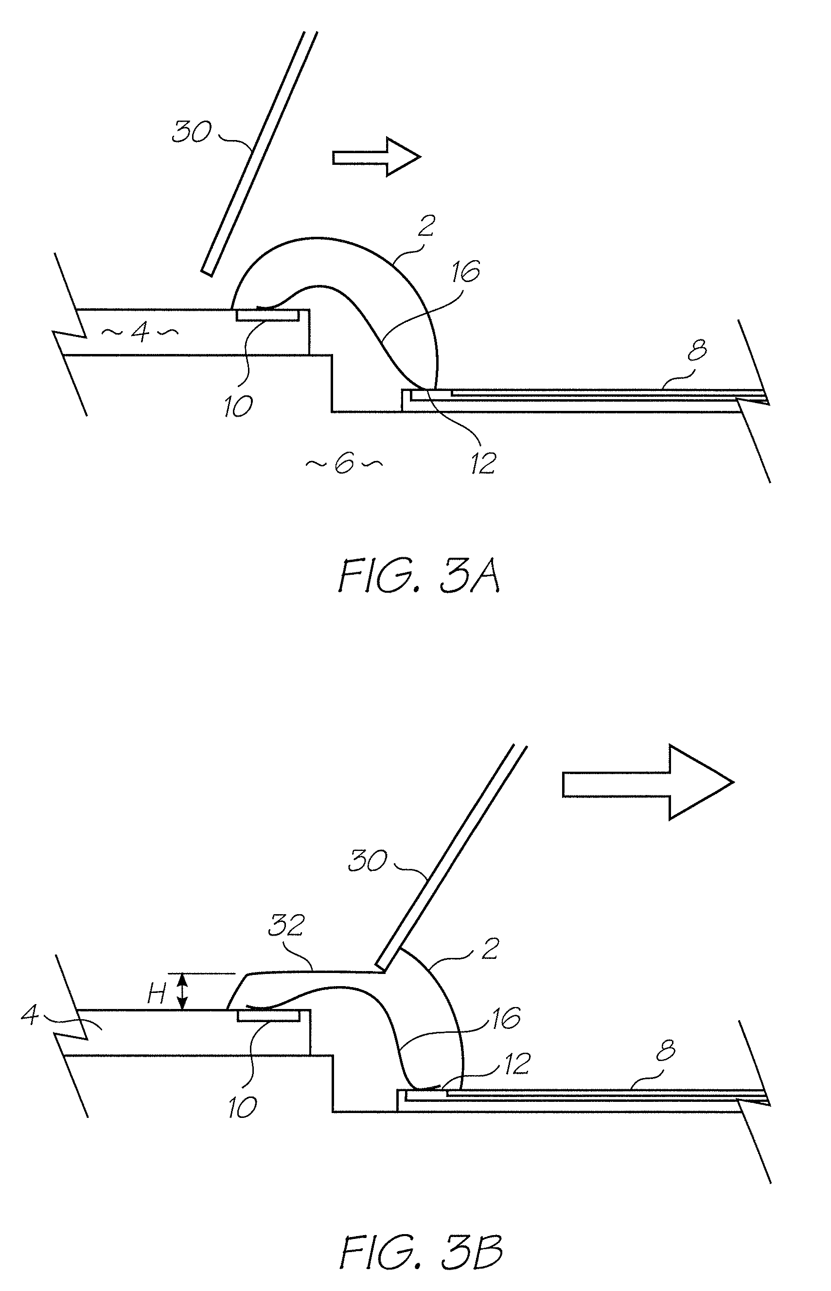
The present invention provides a microprocessor device with a raised chip mounting area and a conductor mounting area, where a chip is supported on the chip mounting area and a flexible printed circuit board with conductors is supported on the conductor mounting area. The chip mounting area is raised relative to the conductor mounting area, allowing the top of the chip to be closer to the active surface of the chip. This reduces the profile of the encapsulant bead, which makes it easier to bring the nozzles of a printhead into close proximity with another surface without making contact. The wire bonds connecting the chip to the flexible printed circuit board are plastically deformed, and a bead of encapsulant is applied over the wire bond to further reduce the profile of the encapsulant bead. The method also includes steps of pushing on the wire bond to collapse the arc and plastically deform the wire bond, and releasing the wire bonds to maintain the wire bond in a flatter profile shape. The strength of the wire bond is relatively small, but the method provides a way to deform the wire bond into a flatter profile without compromising the electrical connection with the printed circuit board.

Problems solved by technology

Similarly, if a cleaning surface is wiped across the nozzles, the bead of encapsulant can hamper the wiping contact.
Another problems arises because of sides of the encapsulant bead are not straight.
The encapsulant volume and placement on the die is not very accurate.
Variations in the pressure from the pump or slight non-uniformities in the speed of the needle cause the side of the bead contacting the active surface to be reasonably crooked.

Method used


Image

  • Method of reducing wire bond profile height in integrated circuits mounted to circuit boards
  • Method of reducing wire bond profile height in integrated circuits mounted to circuit boards
  • Method of reducing wire bond profile height in integrated circuits mounted to circuit boards

Examples


Embodiment Construction

[0122]FIG. 1 shows a common technique used for applying a bead encapsulant to wire bonds. A die 4 is mounted to a supporting structure 6 adjacent the edge of a flex PCB 8 (flexible printed circuit board). The die 4 has a line of contact pads 10 along one edge and the flex PCB 8 has corresponding bond pads 12. Wire bonds 16 extend from the bond pads 10 to the bonds pads 12. Power and data is transmitted to the die 4 via conductive traces 14 in the flex PCB 8. This is a simplified representation of the dies mounted within many electronic devices. The printhead IC dies mounted to the LCP (liquid crystal polymer) molding to receive print data from an adjacent flex PCB, as described in U.S. Ser. No. 11 / 014,769 (grant U.S. Pat. No. 7,524,016) incorporated herein by cross reference, is one example of this type of die mounting arrangement. The ordinary worker will appreciate that the die may also be mounted directly to a hard PCB with traces formed thereon.

[0123]The wire bonds 16 are covere...


PUM

PropertyMeasurementUnit
diameteraaaaaaaaaa
diameteraaaaaaaaaa
diameteraaaaaaaaaa

Abstract

A method of profiling a wire bond between a contact pad on a die, and a conductor on a supporting structure, by electrically connecting the contact pad on the die to the conductor on the supporting structure with a wire bond, the wire bond extending in an arc from the contact pad to the conductor, pushing on the wire bond to collapse the arc and plastically deform the wire bond, and then releasing the wire bonds such that the plastic deformation maintains the wire bond in a flatter profile shape. The strength of the wire bond is known to be relatively small; of the order of 3 to 5 grams force. However, the Applicant's work has found that the wire bond structure is robust enough to withstand a certain degree of work hardening from plastic deformation. The arc of the wire bond can be deformed into a flatter profile without compromising the electrical connection with the PCB.

Description

FIELD OF THE INVENTION[0001]The invention relates to the field of integrated circuit packaging. In particular, the encapsulation of the wire bonds between a circuit board and the contact pads on the integrated circuit die.CO-PENDING APPLICATIONS[0002]The following applications have been filed by the Applicant simultaneously with the present application:[0003]11860538118605401186054111860542[0004]The disclosures of these co-pending applications are incorporated herein by reference.CROSS REFERENCES TO RELATED APPLICATIONS[0005]Various methods, systems and apparatus relating to the present invention are disclosed in the following U.S. Patents / Patent Applications filed by the applicant or assignee of the present invention:[0006]6,405,0556,628,4307,136,18610 / 920,3727,145,6897,130,0757,081,9747,177,0557,209,2577,161,7157,154,6327,158,2587,148,9937,075,6847,158,80911 / 225,17211 / 474,28011 / 635,48211 / 635,52611 / 650,54511 / 653,24111 / 653,24011,758,6487,241,0057,108,4376,915,1406,999,2067,136,1987,...

Claims


Application Information

Patent Timeline
Patent Type & Authority Patents(United States)
IPC IPC(8): B21D39/00
CPCH01L21/56H01L24/48H01L24/78H01L24/85H01L23/3157H01L2924/01006H01L2224/45015H01L2224/4809H01L2224/48091H01L2224/48227H01L2224/48472H01L2224/78H01L2224/8592H01L2224/85947H01L2924/01014H01L2924/01027H01L2924/01033H01L2924/09701H01L2924/14H01L2924/20753H01L2924/1461H01L2924/10253H01L2924/00014H01L2924/20752H01L2924/00H01L2224/85205H01L2224/45099H01L2924/20754H01L2224/05599
Inventor CHUNG-LONG-SHAN, LAVALTANKONGCHUMRUSKUL, KIANGKAISILVERBROOK, KIA
Owner SILVERBROOK RES PTY LTD
Learn More