
Multichip light emitting diode package

a light-emitting diode and multi-chip technology, applied in the direction of basic electric elements, electrical equipment, semiconductor devices, etc., can solve the problems of multi-chip light-emitting diode packages that cannot provide uniform white light, multi-chip light-emitting diode packages cannot provide uniform brightness and hues, etc., to achieve improved brightness and hues, and improve heat dissipation

Inactive Publication Date: 2011-08-02
ADVANCED OPTOELECTRONIC TECH INC
View PDF5 Cites 35 Cited by
  • Summary
  • Abstract
  • Description
  • Claims
  • Application Information

AI Technical Summary

Benefits of technology

[0016]It is another objective of the present invention to provide a multichip light emitting diode package, which can be fabricated to a single color light LED package or a multi-color or a full color light LED package with improved brightness and hues.
[0017]It is a further objective of the present invention to provide a multichip light emitting diode package, in which a heat sink is disposed under the substrate of the LED package to improve heat dissipation.
[0018]It is still a further objective of the present invention to provide a multichip light emitting diode package, which electrically couples with an electro-static protective device to prevent the LEDs from damage by the static discharge.

Problems solved by technology

The white light multichip light emitting diode package cannot provide uniform white light.
The conventional multichip light emitting diode package structure as above cannot provide illuminating light with uniform brightness and hues.
The illumination quality of them is adversely influenced.
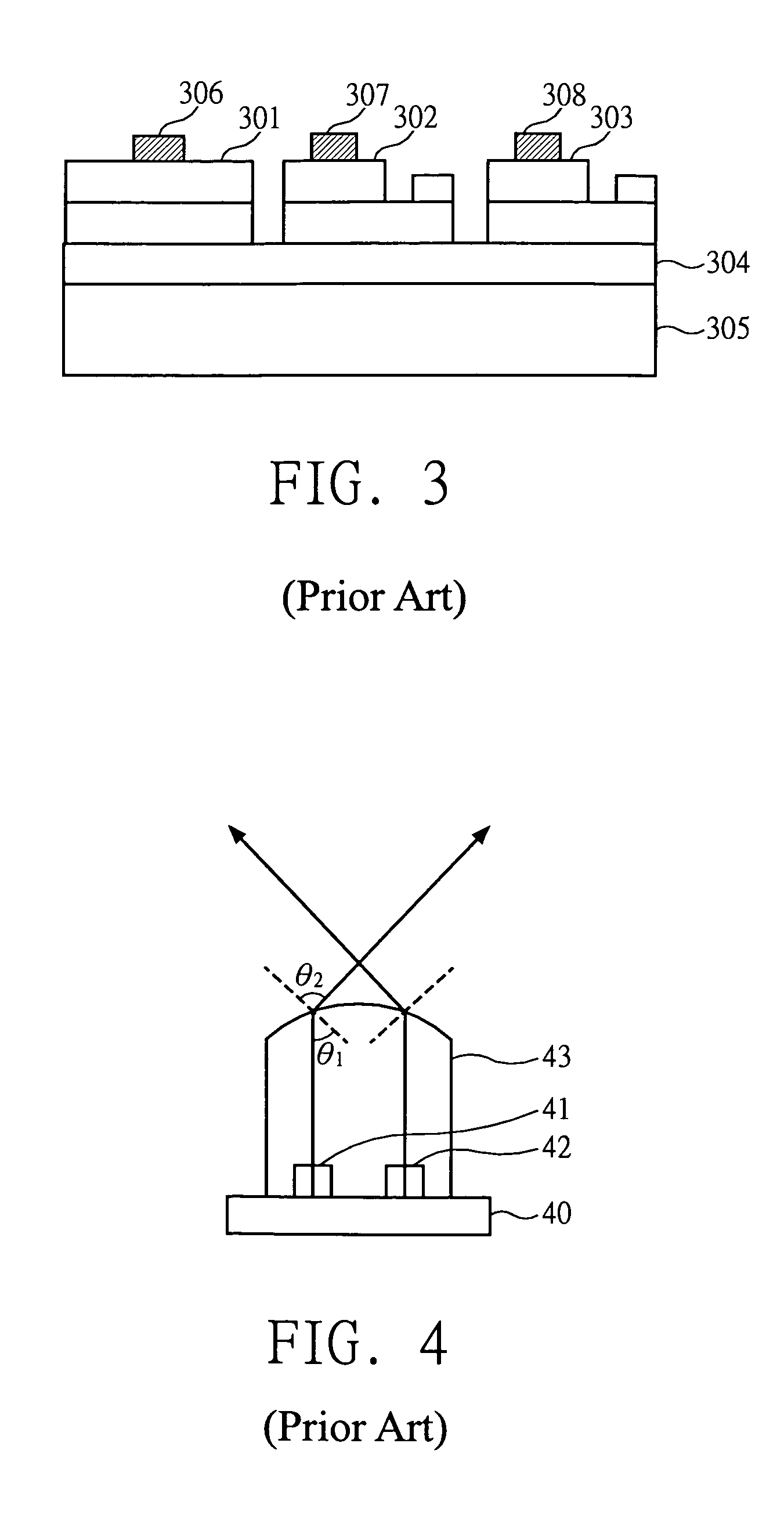
However, it is difficult to form the double dome-shaped epoxy mold 63 by mold injection.
And, it is not easy to control the illumination of the two LED chips 61 and 62 to attain consistence.

Method used


Image

  • Multichip light emitting diode package
  • Multichip light emitting diode package
  • Multichip light emitting diode package

Examples


first embodiment

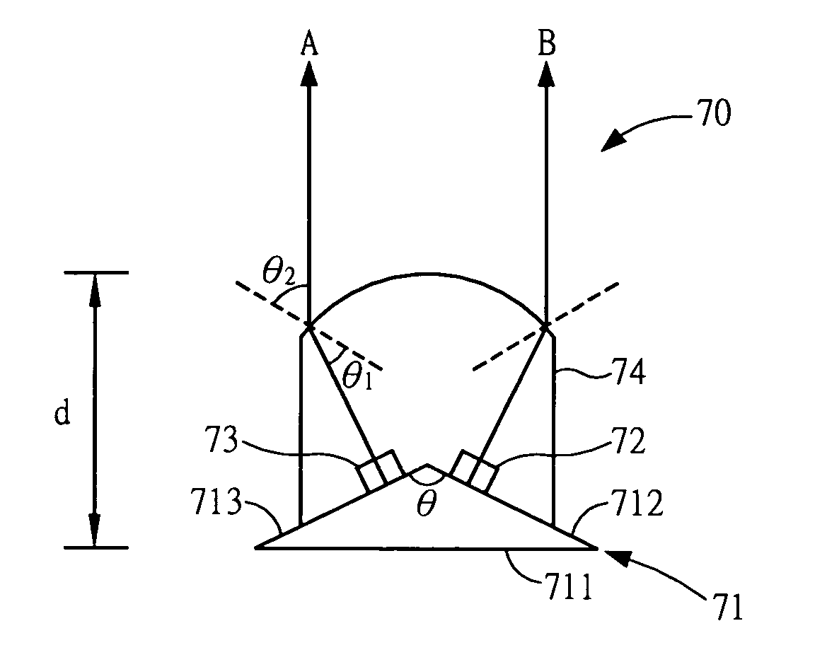
[0043]FIG. 7 is a schematic cross-sectioned view of a multichip light emitting diode package 70 according to the present invention. The multichip light emitting diode package 70 includes a wiring circuit board 71, two LED chips 72 and 73 and a dome-shaped transparent molding material 74. The wiring circuit board 71 includes an upper surface formed of two opposite inclined sides 712 and 713 and a base 711. The traverse cross section of the upper surface has an inversed V-shaped configuration. The wiring circuit board 71 can be a printed circuit board. Each of the LED chips 72 and 73 is respectively disposed on one of the two opposite inclined sides 712 and 713. The LED chips 72 and 73 can be same color LED chips or different color LED chips. The dome-shaped transparent molding material 74 is formed on the wiring circuit board 71 for encapsulating the two LED chips 72 and 73. The transparent molding material 74 can be a transparent resin material, for example a transparent epoxy mater...

second embodiment

[0047]FIG. 8 is a schematic cross-sectioned view of a multichip light emitting diode package 80 according to the present invention. The multichip light emitting diode package 80 includes a wiring circuit board 81, two LED chips 82 and 83 and a dome-shaped transparent molding material 84. The wiring circuit board 81 includes an upper surface formed of two opposite inclined sides 812 and 813 and a base 811. The traverse cross section of the upper surface has a V-shaped configuration. The wiring circuit board 81 can be a printed circuit board. Each of the LED chips 82 and 83 is respectively disposed on one of the two opposite inclined sides 812 and 813. The LED chips 82 and 83 can be same color LED chips or different color LED chips. The dome-shaped transparent molding material 84 is formed on the wiring circuit board 81 for encapsulating the two LED chips 82 and 83. The transparent molding material 84 can be a transparent resin material, for example a transparent epoxy material.

[0048]...

third embodiment

[0051]FIG. 9 is a schematic cross-sectioned view of a multichip light emitting diode package 90 according to the present invention. The multichip light emitting diode package 90 includes a wiring circuit board 91, three LED chips 92, 93 and 94 and a dome-shaped transparent molding material 95. The wiring circuit board 91 includes an upper surface formed of three sectioned-surfaces 912, 913 and 914 and a base 911. The traverse cross section of the upper surface has an inversed trapezoid configuration. The wiring circuit board 91 can be a printed circuit board. Each of the three LED chips 92, 93 and 94 is respectively disposed on one of the three sectioned-surfaces 912, 913 and 914. The three LED chips 92, 93 and 94 can be same color LED chips or different color LED chips, like red LED chip, green LED chip and blue LED chip. The dome-shaped transparent molding material 95 is formed on the wiring circuit board 91 for encapsulating the three LED chips 92, 93 and 94. The transparent mold...


PUM


Abstract

A multichip light emitting diode package is provided. The multichip light emitting diode (LED) package includes a substrate having a non-plane surface including a plurality of sectioned-surfaces, a plurality of light emitting diode chips and a transparent molding material. Each of the light emitting diode chips is disposed on one of the sectioned-surfaces of the substrate. The transparent molding material is formed on the substrate for encapsulating the light emitting diode chips. By way of the configurations of the non-plane surface of the substrate and the transparent molding material, the multichip light emitting diode package emits converging light in accordance with the Snell's law. The purposes of evenly mixing emitting lights and improving brightness are achieved. The present invention can provide a single color, multi-color or full-color multichip LED package with uniform brightness and hues.

Description

BACKGROUND OF THE INVENTION[0001]1. Field of the Invention[0002]The present invention relates to a multichip light emitting diode (LED) package, and more particularly to a multichip light emitting diode package with a substrate having a non-plane surface including a plurality of sectioned-surfaces for disposing LEDs.[0003]2. Description of the Prior Art[0004]As a good light source and device made by semiconductor material, LEDs possess advantages of small size, long life-time, low driving voltage, rapid response, and good oscillation-proof, etc.[0005]By changing the semiconductor materials and device structures, LEDs with different visible and invisible colors can be designed, wherein AlGaAs, InGaAlP and InGaN are suitable for producing LEDs with high luminance over 1000 mcd.[0006]When producing red or infrared LEDs with high luminance by AlGaAs, an LPE process and DE structure devices are used for industrial mass production.[0007]InGaAlP can be used to produce red, orange, yellow a...

Claims


Application Information

Patent Timeline
Patent Type & Authority Patents(United States)
IPC IPC(8): H01L33/00
CPCH01L25/0753H01L2924/0002H01L2924/00
Inventor HSU, CHIH-PENG
Owner ADVANCED OPTOELECTRONIC TECH INC
Learn More