Semiconductor device

a technology of semiconductor and resistor, which is applied in the direction of pulse manipulation, pulse technique, instruments, etc., can solve the problems of voltage drop across, voltage drop across, and the small resistance value of /b> can still become too large to be neglected, so as to improve load characteristics, increase the phase margin of the voltage regulator, and reduce the effect of voltage loss

Inactive Publication Date: 2011-08-02
RICOH ELECTRONIC DEVICES CO LTD
View PDF12 Cites 0 Cited by
  • Summary
  • Abstract
  • Description
  • Claims
  • Application Information

AI Technical Summary

Benefits of technology

[0040]In the above-mentioned semiconductor devices, since the semiconductor chip having a voltage regulator and a phase compensation condenser for phase compensation of the voltage regulator, or a phase compensation resistor connected to the phase compensation condenser in series, can be accommodated in a single package, such as a CSP, an external part and mounting step can be omitted; further, inventory control of the phase compensation condenser can be omitted on the side of users. In addition, since it is possible to perform inspection and quality assurance with the condenser being mounted, it is possible to improve operational stability and quality, and obtain an easy-to-use voltage regulator.
[0046]In addition, since the phase compensation resistor may have a resistance from 10 mΩ to 1.5Ω, it is possible to perform phase compensation of the voltage regulator easily, and obtain a voltage regulator of high stability.

Problems solved by technology

Due to the different equivalent series resistances of condensers connected to the output terminal, sometimes phase compensation of the voltage regulator cannot be performed appropriately depending on types of the condensers.
When the ceramic condenser, which has a small equivalent series resistance, is connected to the voltage regulator, however, the above-mentioned zero-point in the frequency characteristic curve moves to the high frequency side, the phase margin disappears in the region where the frequency gain is near 0 dB, and this causes oscillation.
Because of such an output condenser C121, the phase margin may become small, and furthermore, in applications involving large currents, the voltage drop across the resistor R113 having such a small resistance value can still become too large to be neglected.
Due to this, quality and ease of use of the device cannot be improved sufficiently.

Method used


Image

  • Semiconductor device
  • Semiconductor device
  • Semiconductor device

Examples


first embodiment

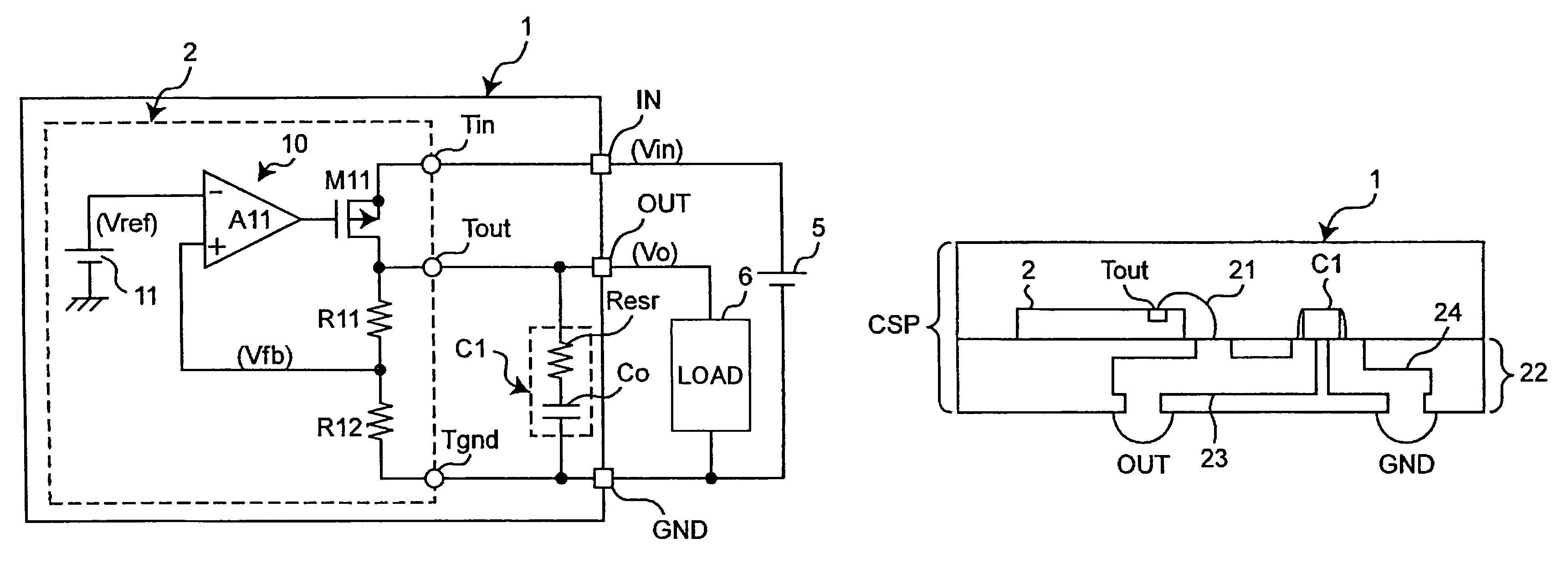
[0060]FIG. 1 is a circuit diagram illustrating an example of a semiconductor device according to a first embodiment of the present invention.

[0061]In a semiconductor device 1 shown in FIG. 1, a semiconductor chip 2 having a voltage regulator 10, and an output condenser C1 are installed in a chip-size package (CSP). The semiconductor device 1 further includes a power supply input terminal IN, an output terminal OUT, and a ground terminal GND connected to ground potential. An input voltage Vin from a direct current power supply 5 is input to the power supply input terminal IN. The output condenser C1 serves as the phase compensation condenser of the voltage regulator 10. An output voltage Vo from the voltage regulator 10 is supplied to a load 6 through the output terminal OUT.

[0062]The voltage regulator 10 constitutes a series regulator, which transforms the input voltage Vin supplied to the power supply input terminal IN to a specified constant voltage, and outputs the output voltage...

second embodiment

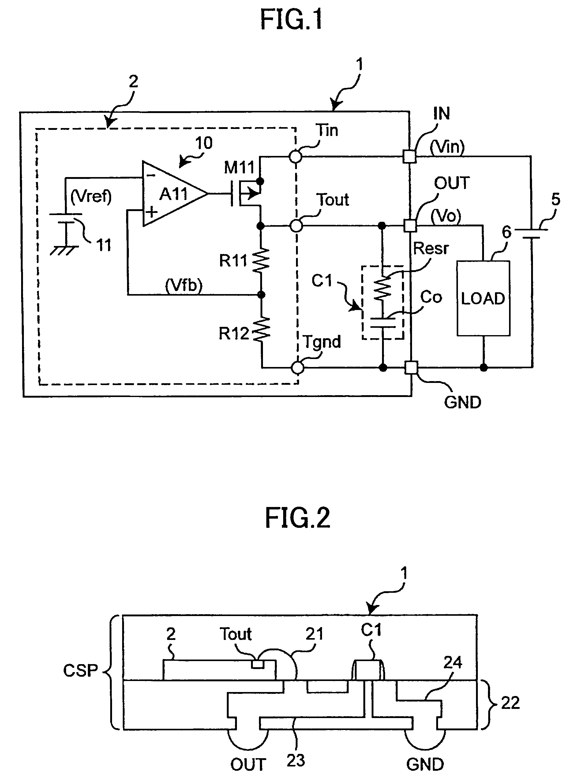
[0069]FIG. 3 is a circuit diagram illustrating an example of a semiconductor device according to a second embodiment of the present invention.

[0070]In FIG. 3, the same reference numbers are assigned to the same elements as those described previously, and overlapping descriptions are omitted.

[0071]A semiconductor device 1a in FIG. 3 differs from the semiconductor device 1 in FIG. 1 in that a resistor R13 is disposed for adjusting ESR of the output condenser C1.

[0072]In the semiconductor device 1a as shown in FIG. 3, a semiconductor chip 2, an output condenser C1, and the resistor R13 for adjusting the ESR of the output condenser C1 are installed in the chip-size package (CSP). The resistor R13 serves as the phase compensation resistor. A serial circuit of the resistor R13 and the output condenser C1 is connected between the connection point of the output terminal Tout of the semiconductor chip 2 and the output terminal OUT of the CSP, and the connection point of the ground terminal T...

third embodiment

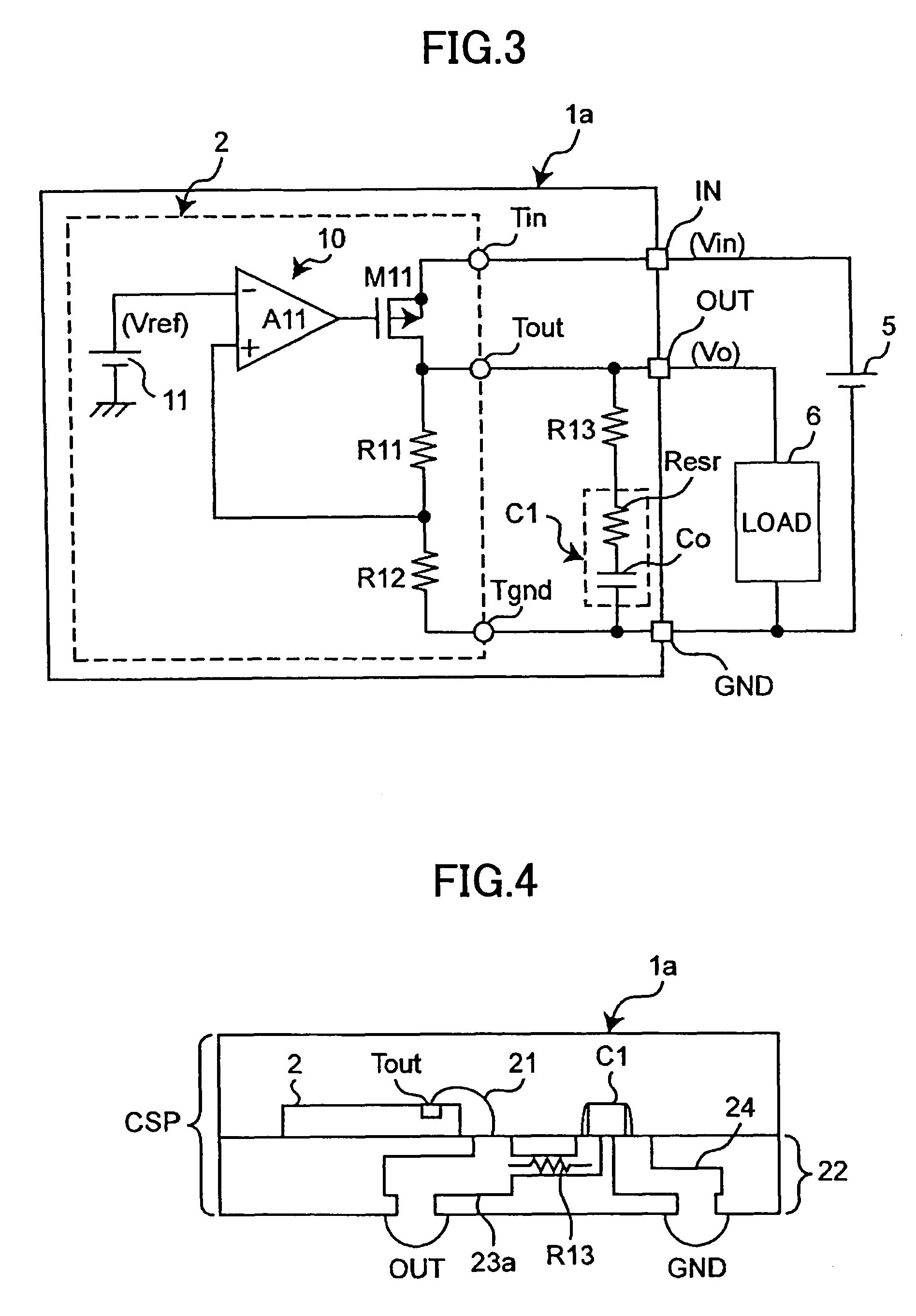
[0083]In the previous embodiment, the phase compensation resistor (resistor R13) is disposed in the CSP, but the phase compensation resistor may also be disposed in the semiconductor chip.

[0084]FIG. 5 is a circuit diagram illustrating an example of a semiconductor device according to a third embodiment of the present invention.

[0085]In FIG. 5, the same reference numbers are assigned to the same elements as those described previously, and overlapping descriptions are omitted.

[0086]In the present embodiment, the resistor R13 is disposed in a semiconductor chip 2a, instead of in the CSP. In addition, a connection terminal Ta is formed in the semiconductor chip 2a for connecting the output condenser C1 and the resistor R13.

[0087]In the semiconductor device 1b as shown in FIG. 5, a semiconductor chip 2b having a voltage regulator 10 and the output condenser C1 are installed in the CSP.

[0088]The semiconductor chip 2b includes the voltage regulator 10 and the resistor R13, the power supply...


PUM


Abstract

A semiconductor device having a voltage regulator is disclosed that does not have an external output condenser for phase compensation. The semiconductor device includes a semiconductor chip that includes a voltage regulator, a power supply input terminal, a ground terminal, and an output terminal for outputting a produced constant voltage; and a phase compensation condenser that is connected between the output terminal and the ground terminal for phase compensation of the voltage regulator. The semiconductor chip and the phase compensation condenser are accommodated in a single package.

Description

TECHNICAL FIELD[0001]The present invention relates to a semiconductor device in which an IC chip having a voltage regulator is installed in a chip-size package (CSP: Chip Size Package), and particularly, to a semiconductor device having a voltage regulator with a condenser connected between an output terminal and a grounding terminal of the voltage regulator for phase compensation.BACKGROUND ART[0002]In the related art, in an IC chip including a voltage regulator, an output condenser is connected to an output terminal of the voltage regulator parallel to a load. Generally, an electrolytic condenser or a tantalum condenser is used as the output condenser, but recently, a stacked ceramic condenser, which is compact and able to have a large capacity, has been developed and put into practical use.[0003]The electrolytic condenser, the tantalum condenser, and the stacked ceramic condenser have different equivalent series resistances (abbreviated to be “ESR” where necessary). For example, ...

Claims


Application Information

Patent Timeline
Patent Type & Authority Patents(United States)
IPC IPC(8): H01L23/02
CPCG05F1/56H01L2224/48091H01L2924/15192H01L2924/15311H01L2924/19105H01L2924/00014H01L25/04
Inventor ITOH, KOHZOH
Owner RICOH ELECTRONIC DEVICES CO LTD
Why Eureka
Try Eureka