
Class queue for network data switch to identify data memory locations by arrival time
a network data switch and data memory technology, applied in the field of network switches, can solve the problem that the pci express switch will not support other protocols or standards, and achieve the effect of preventing collisions on data read out and ensuring latency
- Summary
- Abstract
- Description
- Claims
- Application Information
AI Technical Summary
Benefits of technology
Problems solved by technology
Method used
Image

Examples
Embodiment Construction
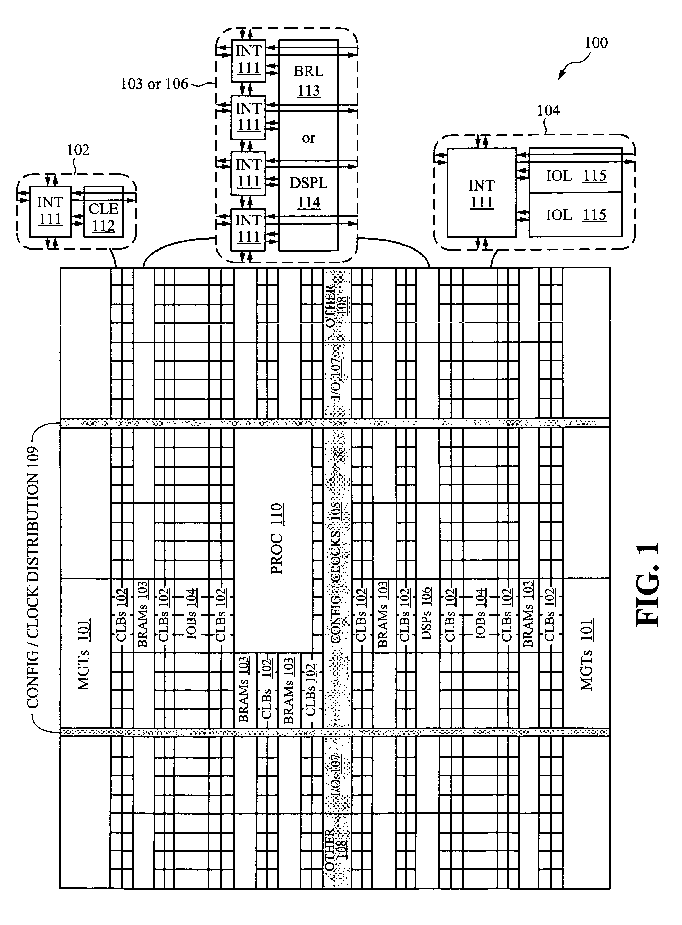
[0023]Embodiments of the present invention are described for use in an FPGA. The network switch according to the present invention provides for communications between nodes or modules programmed into the logic of an FPGA. The network switch is also programmed into the logic. Further, the FPGA memory can be configured to meet the parameters defined for the switch. Although the following description of embodiments of the present invention are described with respect to particular components of an FPGA, it is understood that other integrated circuits with on board programmable logic and memory can be programmed to include a network switch according to embodiments of the present invention. For reference, FIG. 1 shows one configuration of components of an FPGA that can be configured to include a network switch according to the present invention.
FPGA Overview
[0024]The FPGA of FIG. 1 includes a large number of different programmable tiles including MGTs 101, configurable logic blocks (CLBs ...
PUM
 Abstract
Description
Claims
Application Information