Method of stitching scan flipflops together to form a scan chain with a reduced wire length

a technology of scan flipflops and scan chains, applied in pulse generators, pulse techniques, instruments, etc., can solve the problems of difficult to test scan flipflops, inability to easily test scan flipflops, and extremely complex logic functions of cmos chips

Active Publication Date: 2011-08-09
NAT SEMICON CORP
View PDF45 Cites 7 Cited by
  • Summary
  • Abstract
  • Description
  • Claims
  • Application Information

AI Technical Summary

Problems solved by technology

Many modern day CMOS chips contain extremely complex logic functions.
As a result, it is very difficult to test these chips because they often contain many thousands of flipflops that can assume many millions of logic states.
A serious shortcoming of flipflop 100 in FIG. 1 is that it cannot be easily tested.
In other words, the flipflop output cannot be easily controlled (forced high or low) because the flipflop input DIN is connected to internal logic gates.
As a consequence of this, flipflop 100 cannot be directly driven by on-chip test logic.
If the two vectors do not match, the chip is said to be ‘bad’.
In this case, the chip test fails, and the chip is bad.
Furthermore, the standard cell rows can be touching each other, or they can be non-uniformly spaced apart.
As a result of this wire routing, the scan chain wires can become long and congested.
The scan stitching shown in FIG. 6 is highly undesirable for a number of reasons.
Firstly, it forces the scan chain wires to make unnecessary (and often substantial) traverses in the horizontal and vertical directions.
Furthermore, these unnecessary wire traverses are bad because they can substantially increase the lengths and congestion of the scan chain wires, unnecessarily increasing the capacitance on the scan flip-flop outputs.
In addition, the capacitance increase on the scan flipflop outputs can also decrease the chip operating speed.
Furthermore, the unnecessary scan wire traverses also force the router to make unnecessary metal layer changes, when routing a given scan chain.
Moreover, these unnecessary metal layer changes often generate pieces of scan chain wire on several different metal layers.
As a consequence of this, these pieces of scan chain wire can easily block the routing of non-scan nets, in those regions where the pieces of scan chain wire exist.
In other words, the wire congestion in these regions will be increased, which can easily cause the chip size to increase.

Method used


Image

  • Method of stitching scan flipflops together to form a scan chain with a reduced wire length
  • Method of stitching scan flipflops together to form a scan chain with a reduced wire length
  • Method of stitching scan flipflops together to form a scan chain with a reduced wire length

Examples


Embodiment Construction

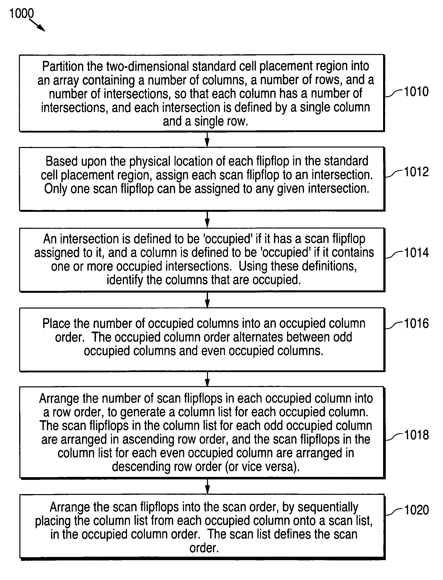
[0054]In accordance with the present invention, FIG. 7 shows a flow chart that illustrates an example of a method 700 of stitching scan flip-flops together. As described in greater detail below, the method of the present invention substantially improves the scan stitching order for the scan flipflops in a scan chain.

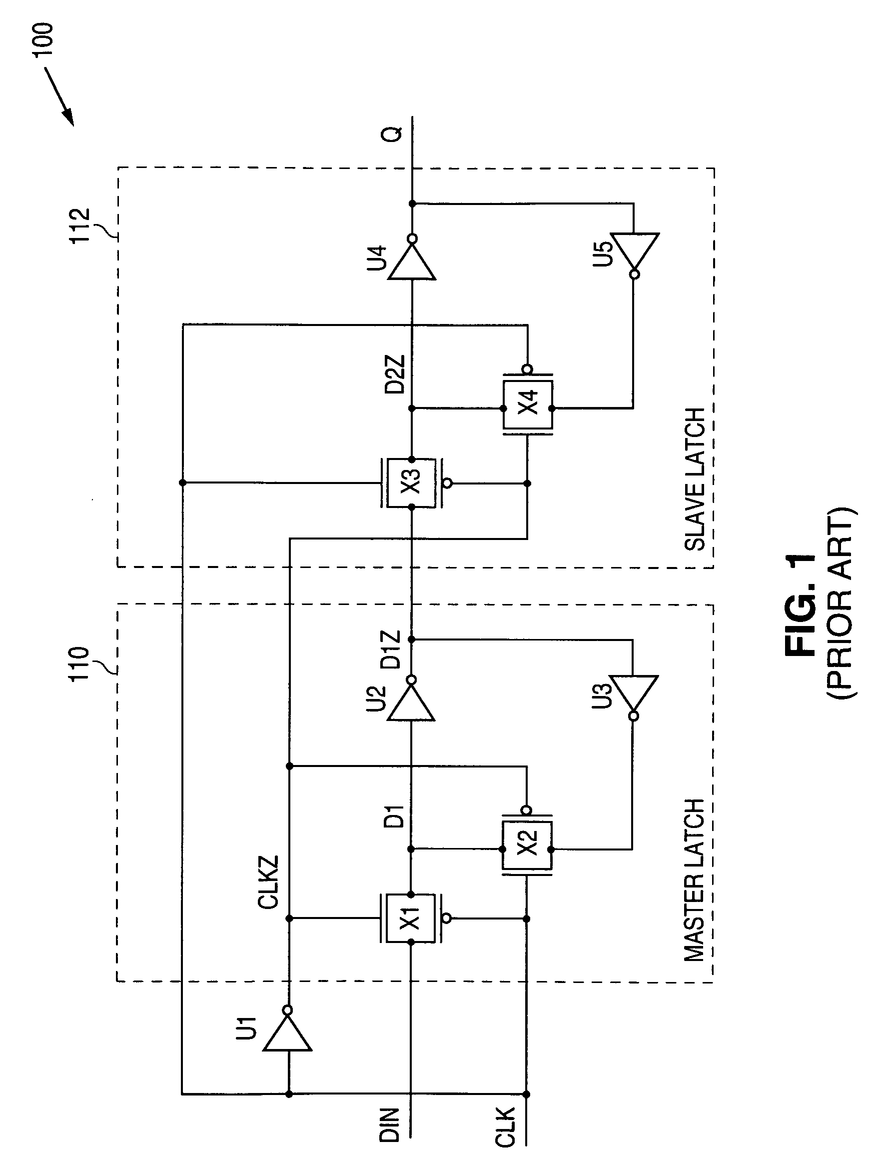
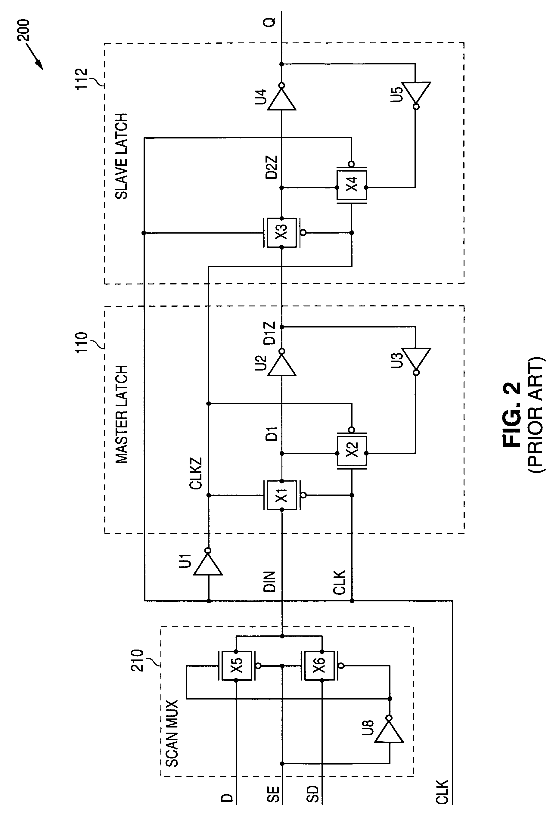
[0055]Before discussing method 700, the following terms are first defined. A netlist is a file that contains interconnect information for standard cells, and / or macro blocks, and / or I / O cells. A Verilog netlist is a netlist that is in Verilog format. A chip-level or top-level netlist is a netlist for an entire chip. The netlist can contain standard cells, macro blocks and I / O cells. An unstitched netlist is a netlist that contains scan flipflops whose SD and SE pins are not connected. A stitched netlist is a netlist that contains scan flipflops whose SD and SE pins are connected.

[0056]A D flipflop is a flipflop that does not contain SD and SE scan pins. A scan flipflop i...


PUM


Abstract

The scan flipflops on a semiconductor chip are stitched together to form one or more scan chains, located in one or more standard cell placement regions, after the optimal physical location of each scan flip-flop has been determined. As a result, the total length of the scan chain wires is substantially reduced, thereby reducing on-chip wiring congestion, flip-flop load capacitance, and flipflop power dissipation.

Description

BACKGROUND OF THE INVENTION[0001]1. Field of the Invention[0002]The present invention relates to scan chain stitching, and more particularly, to a method of stitching scan flipflops together to form a scan chain with a reduced wire length.[0003]2. Description of the Related Art[0004]Many modern day CMOS chips contain extremely complex logic functions. As a result, it is very difficult to test these chips because they often contain many thousands of flipflops that can assume many millions of logic states. Furthermore, in order to efficiently test a chip, the logic states of the chip must be easily controllable and observable. In other words, all of the flipflop outputs on a chip must be easily controllable, and these same outputs must also be easily observable. This controllability / observability, in turn, allows a complex state-dependent test problem to be reduced to a much simpler combinatorial test problem.[0005]Flipflops are well-known logic elements that receive a data signal and...

Claims


Application Information

Patent Timeline
Patent Type & Authority Patents(United States)
IPC IPC(8): G06F17/50
CPCG01R31/318536G01R31/318575
Inventor PASQUALINI, RONALD
Owner NAT SEMICON CORP
Why Eureka
Try Eureka