Method of minimizing early-mode violations causing minimum impact to a chip design

a technology of early-mode violations and chip design, applied in the field of methods, can solve the problems of reducing the quality of the design with respect to area, power and routability, and the difficulty of correcting early-mode violations, so as to reduce the impact on already completed work, effectively delay the fast path, and optimize the design

Inactive Publication Date: 2011-08-09
MENTOR GRAPHICS CORP
View PDF19 Cites 17 Cited by
  • Summary
  • Abstract
  • Description
  • Claims
  • Application Information

AI Technical Summary

Benefits of technology

[0020]Accordingly, it is an object of the present invention to provide a system and a method for correcting early-mode timing violations in chip circuit design while minimizing disruptions to other design characteristics.
[0022]It is a further object to optimize the timing by correcting the early-mode violations without padding fast paths to slow them down by increasing the path delay of the fast paths, and for performing the optimizations while reducing the design impact.
[0024]It is a still a further object to provide a system and method that optimizes the design by effectively delaying the fast paths, while minimizing the impact on already completed work on the chip.
[0025]In one aspect of the invention, a new class of optimizations for correcting of early-mode timing violations in electronic circuits is described, together with a method of deployment which achieves minimizing the use of delay pads and avoiding design disruptions.
[0026]In another aspect of the invention, there is provided a method and a system for correcting early-mode timing violations in a chip design formed by a plurality of interconnected nets and cells, the chip design having undergone placement, late-mode timing closure, routing, electrical and timing analysis, the method including: selecting at least one of the interconnected nets and cells of the chip design having an early mode slack that is smaller than a predetermined threshold; and performing on at least one of the interconnected nets and cells at least one local optimization other than early mode padding, the local optimization improving the early mode slack.

Problems solved by technology

Correcting early mode violations has become a challenging problem in newer technologies.
When chips become larger with a corresponding increase in density, as guard-banding due to variations becomes more significant, and as clock domains and skew increases, the number of pads that require handling hold violations becomes unmanageable.
The added padding, however, degrades the quality of the design with respect to area, power and routability.
For the late mode, some logic paths may be too slow and as a result, the expected value becomes available one cycle too late.
A single set of setup and hold tests for a node is normally not robust enough to ensure that chip timing achieves zero slack at a variety of different process and operating points.
As chips become larger and denser, guardbanding due to variations increases together with the clock domains and skew, the number of pads that needs to be inserted increases, even though padding can degrade the quality of the design with respect to area, power and routability.
The problem of correcting early-mode violations is well known.
An inherent difficulty when using pads to correct hold violations is that the pads consume both space on the chip image and power, and generally makes wiring the design more difficult.
However, in current and future design environments, hold violations are more numerous as a result of the increasing number of clock domains, increased guard-banding related to process variation, and increased clock skew related to large chip sizes.
In addition, more exacting power constraints and more dense use of silicon make the insertion of many thousands of delay pads problematic.
Moreover, this problem is compounded as a result of continuously advancing technologies.
Area and power constraints make the reliance on only traditional padding techniques problematic.

Method used


Image

  • Method of minimizing early-mode violations causing minimum impact to a chip design
  • Method of minimizing early-mode violations causing minimum impact to a chip design
  • Method of minimizing early-mode violations causing minimum impact to a chip design

Examples


Embodiment Construction

[0038]The accompanying drawings, which are incorporated herein and which constitute part of the specification, illustrate the presently preferred embodiments of the invention which, together with the general description given above and the detailed description of the preferred embodiments given below serve to explain the principles of the invention.

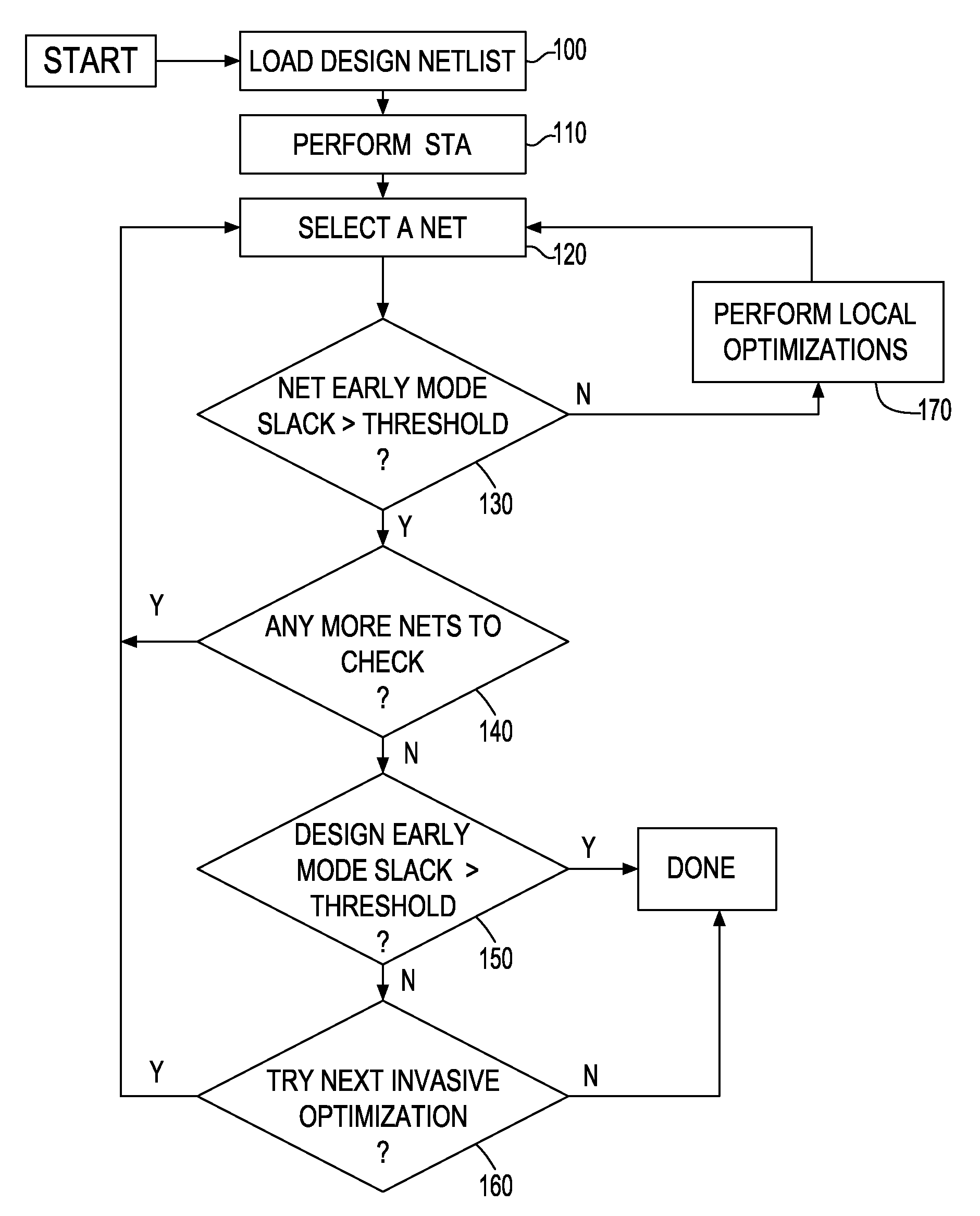
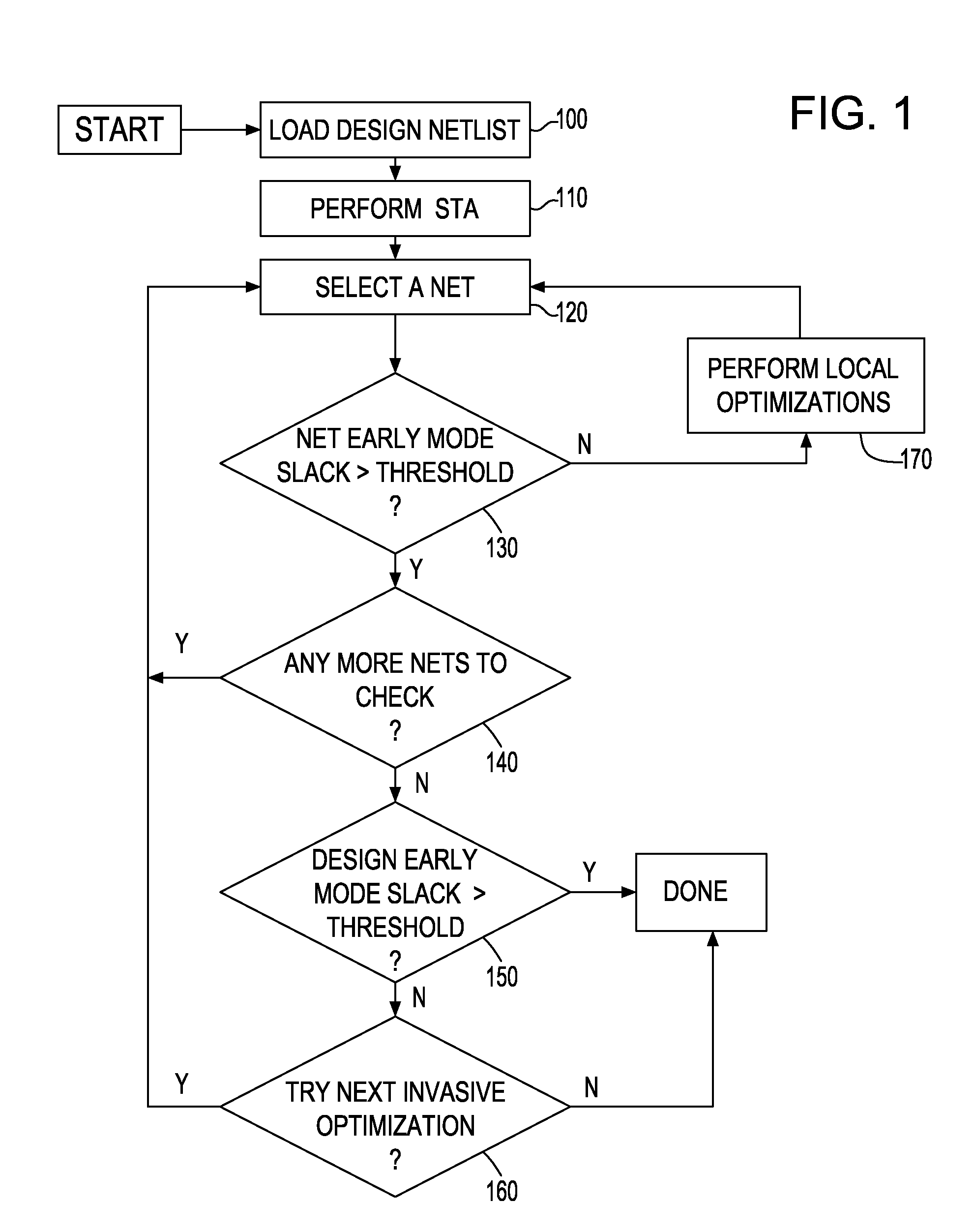
[0039]Referring now to FIG. 1, in one embodiment of the invention, the design optimization or correction process starts by loading a design netlist, step 100. A conventional static timing analysis (STA) is then performed in step 110 using estimated net capacitances or extracted detailed parasitics. In step 120, an iterative process is initiated, checking and correcting nets by selecting a first net on which to operate. The selection may be done by choosing, one by one, all nets of the design, or by restricting the process to nets having a slack that is less than a predetermined threshold. As local optimizations are performed in step 150, ...


PUM


Abstract

A system and a method for correcting early-mode timing violations that operate across the process space of a circuit design. Optimizations are performed to replace padding that increase path delays on fast paths. At the stage in the design process where early-mode violations are addressed, placement, late-mode timing closure, routing, and detailed electrical and timing analysis are assumed to have been completed. The optimizations are designed to be effective in delaying fast paths while minimizing the impact on already-completed work on the chip, in contrast to relying only on adding pads that can have a negative impact on all of these quantities. The optimizations are classified according to their invasiveness and are followed by their deployment. The deployment is designed to minimize using delay pads, reduce design disruptions, and minimize effects on other aspects of the design.

Description

FIELD OF THE INVENTION[0001]The invention generally relates to the field of automating the design of very large scale integrated circuit (VLSI) chips, and more particularly, to a system and a method for improving the timing by detecting and correcting early-mode timing violations in the electronic circuits while minimizing disruptions to other design characteristics.BACKGROUND OF THE INVENTION[0002]Traditionally, early mode violations in electronic circuit designs are corrected late in a design cycle. Correcting early mode violations has become a challenging problem in newer technologies. The most common solution to the fixing early-mode violations is to insert delay cells or pads along the fast paths to slow them down. When chips become larger with a corresponding increase in density, as guard-banding due to variations becomes more significant, and as clock domains and skew increases, the number of pads that require handling hold violations becomes unmanageable. The added padding, ...

Claims


Application Information

Patent Timeline
Patent Type & Authority Patents(United States)
IPC IPC(8): G06F9/455G06F17/50
CPCG06F17/5031G06F2217/84G06F30/3312G06F2119/12
Inventor KOTECHA, POOJA M.MUSANTE, FRANK J.PURESWARAN, VEENA S.TREVILLYAN, LOUISE H.VILLARRUBIA, PAUL G.
Owner MENTOR GRAPHICS CORP
Why Eureka
Try Eureka