
Cell structure for dual port SRAM

a cell structure and dual-port technology, applied in the field of memory cells, can solve problems such as junction leakage and current crowding at the intersection region

Active Publication Date: 2011-08-30
TAIWAN SEMICON MFG CO LTD
View PDF26 Cites 43 Cited by
  • Summary
  • Abstract
  • Description
  • Claims
  • Application Information

AI Technical Summary

Benefits of technology

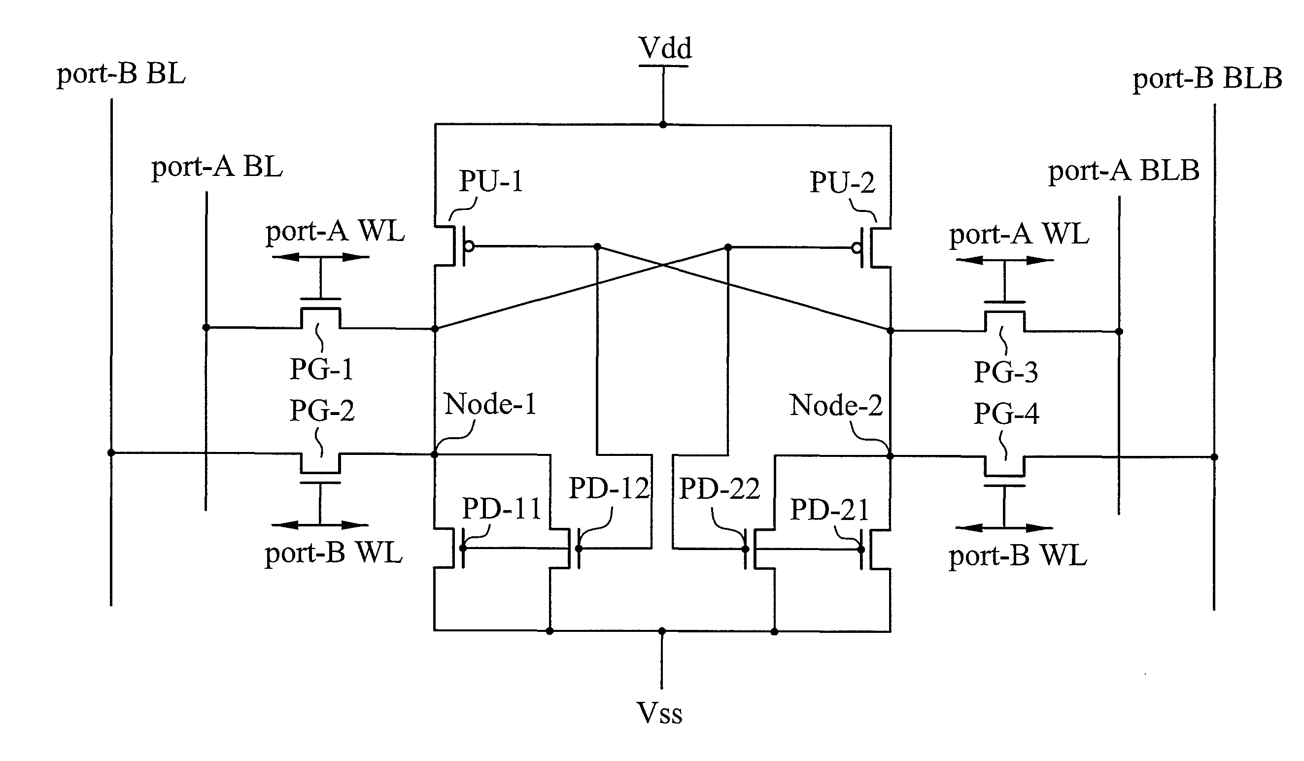
The present invention provides a multi-port SRAM cell with improved performance and reliability. The cell includes first and second cross-coupled inverters with a data storage node and a data bar storage node, each inverter comprising a pull-up transistor and a pull down device. The pull down devices are formed in separate active regions and include at least a pair of pull down transistors. The cell also includes first and second access ports coupled to first and second word line conductors, each access port including a first pass gate transistor and a second pass gate transistor, and a first power supply conductor and a second power supply conductor. The technical effects of the invention include improved data storage and access speed, reduced power consumption, and improved reliability.

Problems solved by technology

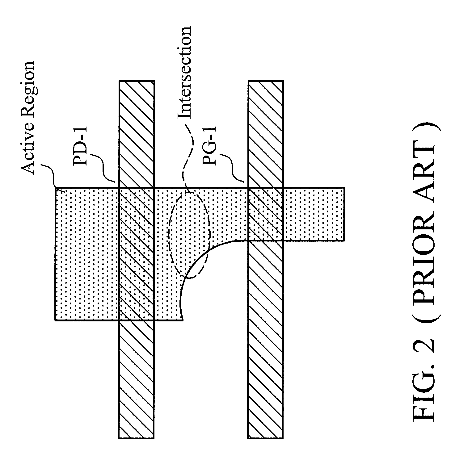
An additional problem is the current crowding at the intersection region.
Junction leakage is also a concern.

Method used


Image

  • Cell structure for dual port SRAM
  • Cell structure for dual port SRAM
  • Cell structure for dual port SRAM

Examples


Embodiment Construction

This description of the exemplary embodiments is intended to be read in connection with the accompanying drawings, which are to be considered part of the entire written description. In the description, relative terms such as “lower,”“upper,”“horizontal,”“vertical,”“above,”“below,”“up,”“down,”“top” and “bottom” as well as derivative thereof (e.g., “horizontally,”“downwardly,”“upwardly,” etc.) should be construed to refer to the orientation as then described or as shown in the drawing under discussion. These relative terms are for convenience of description and do not require that the apparatus be constructed or operated in a particular orientation. Terms concerning attachments, coupling and the like, such as “connected” and “interconnected,” refer to a relationship wherein structures are secured or attached to one another either directly or indirectly through intervening structures, as well as both movable or rigid attachments or relationships, unless expressly described otherwise.

De...


PUM


Abstract

A multi-port SRAM cell includes cross-coupled inverters each including a pull-up transistor and at least a pair of pull down transistors. The SRAM cell includes first and second access ports coupled to first and second word line conductors, each access port including a first pass gate transistor coupled to the data storage node and a second pass gate transistor coupled to the data bar storage node, each pass gate transistor being coupled to a respective bit line conductor, wherein the pull down transistors of the first inverter are formed in a first active region, the pull down transistors of the second inverter are formed in a second active region, the pass gate transistors coupled to the data storage node are formed in a third active region and the pass gate transistors coupled to the data bar storage node are formed in a fourth active region.

Description

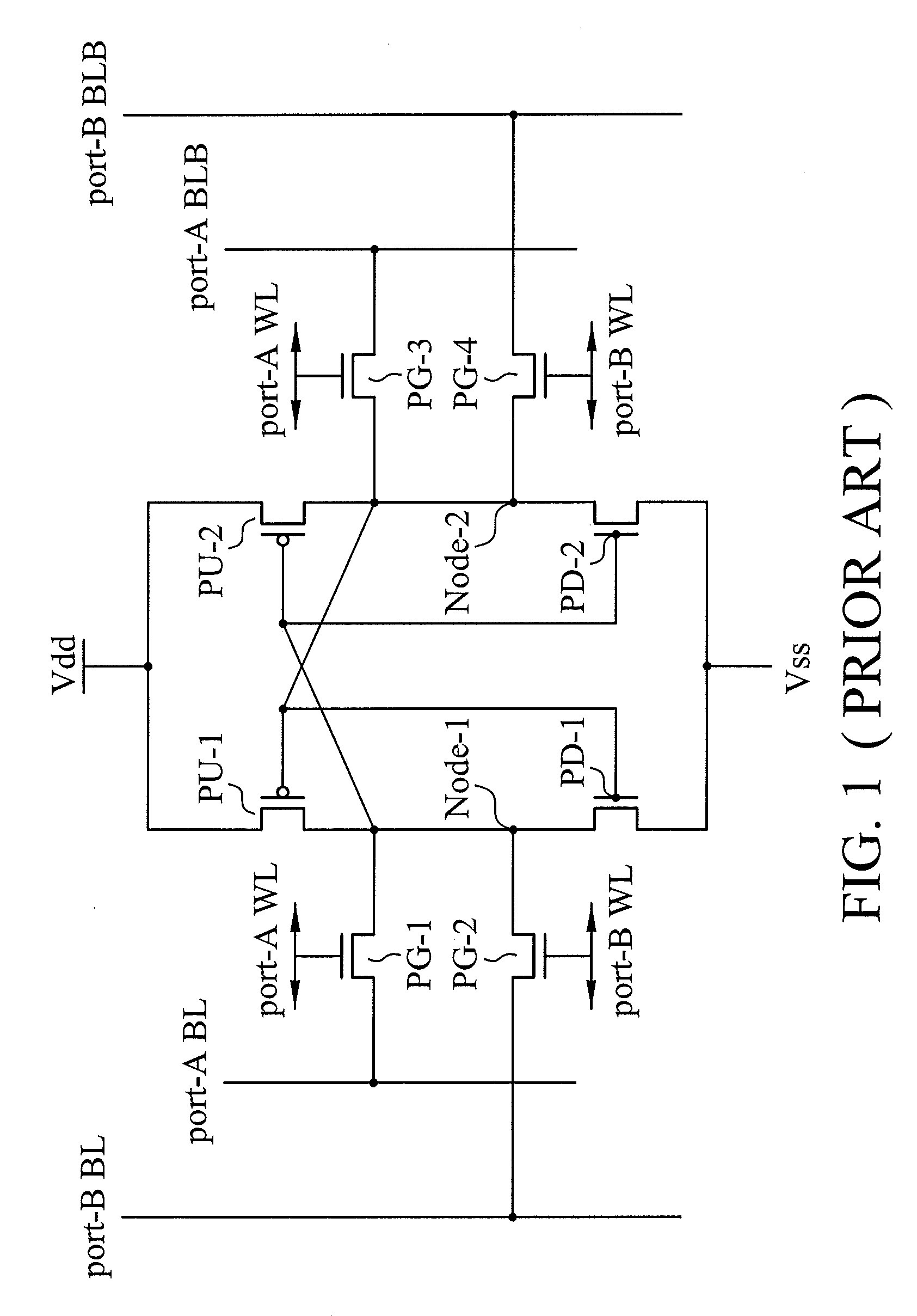
FIELD OF THE INVENTIONThis invention relates generally to semiconductor devices, and more particularly to memory cells, and even more particularly to structures and layout designs of static random access memory cells.BACKGROUND OF THE INVENTIONStatic random access memories (SRAM) are commonly used in integrated circuits. Embedded SRAM is particularly popular in high speed communication, image processing and system on chip (SOC) applications. SRAM cells have the advantageous feature of holding data without requiring a refresh. Typically, a SRAM cell includes two pass-gate transistors, through which a bit can be read from or written into the SRAM cell. This type of SRAM cell is referred to as a single port SRAM cell. Another type of SRAM cell is referred to as dual port SRAM cell, which includes four pass-gate transistors.FIG. 1 illustrates an exemplary circuit diagram of a prior art eight-transistor dual port SRAM cell, which includes pull-up transistors PU-1 and PU-2 and pull-down t...

Claims


Application Information

Patent Timeline
Patent Type & Authority Patents(United States)
IPC IPC(8): G11C11/00
CPCG11C8/16G11C11/412H01L27/0207H10B10/12
Inventor LIAW, JHON JHY
Owner TAIWAN SEMICON MFG CO LTD
Learn More