Magnetic random access memory

a random access and memory technology, applied in the field of magnetic random access memory, can solve the problems of deterioration in data determination reliability, difficult in practice to make voltage vs and voltage vns exactly the same, etc., and achieve the effect of improving selectivity of memory cells at the time of data writing to the mram and improving reliability of read data at the time of data reading from the mram

Active Publication Date: 2011-08-30
NEC CORP
View PDF6 Cites 10 Cited by
  • Summary
  • Abstract
  • Description
  • Claims
  • Application Information

AI Technical Summary

Benefits of technology

[0013]Another object of the present invention is to provide a technique that can improve reliability of a read data at a time of data reading from an MRAM.
[0014]Another object of the present invention is to provide a technique that can improve selectivity of a memory cell at a time of data writing to an MRAM.
[0023]Another effect of the present invention is that the reliability of the read data at the time of data reading from the MRAM is improved.
[0024]Another effect of the present invention is that the selectivity of the memory cell at the time of data writing to the MRAM is improved.

Problems solved by technology

That is, the parallel current causes deterioration in reliability of the data determination for the selected memory cell 120s.
However, it is difficult in practice to make the voltage Vs and the voltage Vns exactly the same.

Method used


Image

  • Magnetic random access memory
  • Magnetic random access memory
  • Magnetic random access memory

Examples


first embodiment

1. First Embodiment

1-1. Circuit Configuration

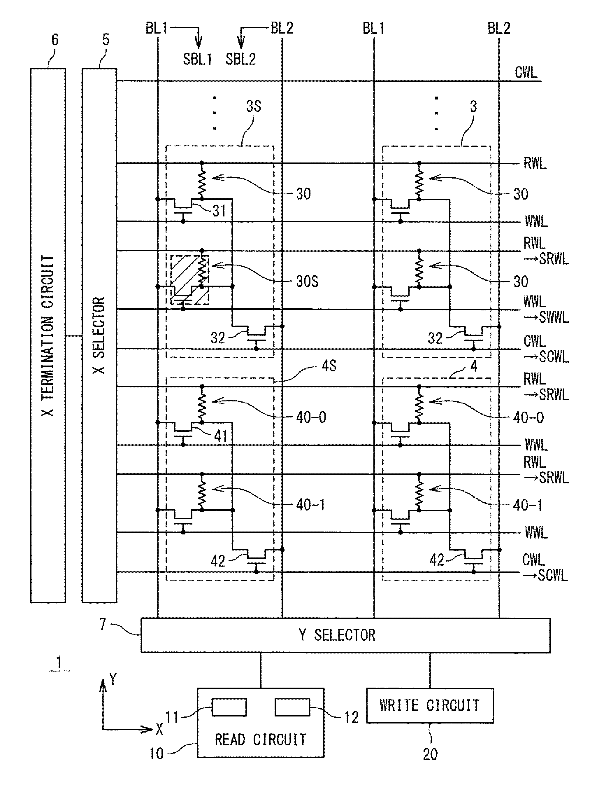
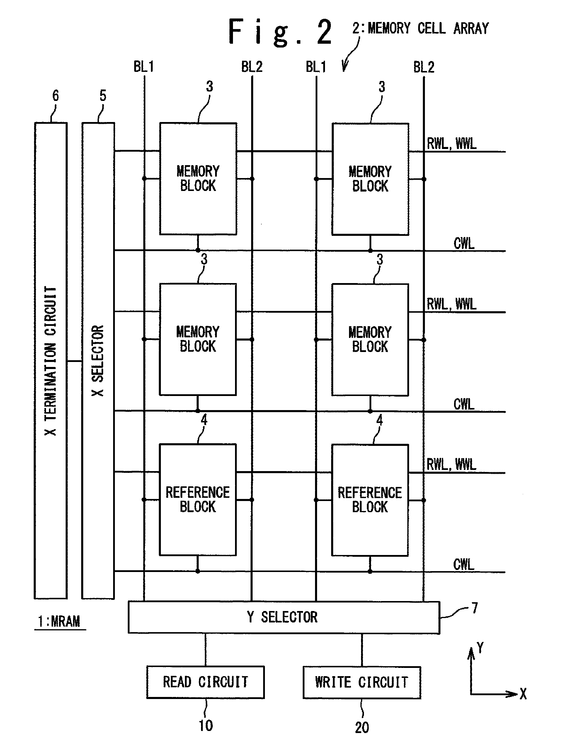
[0064]FIG. 2 is a block diagram schematically showing a configuration of an MRAM in a first embodiment of the present invention. The MRAM 1 is provided with a memory cell array 2 in which a plurality of memory cells are arranged in a matrix form. The memory cell array 2 is sectioned into a plurality of blocks (3, 4). The plurality of blocks are arranged in a matrix form. More specifically, the plurality of blocks include a plurality of memory blocks 3 arranged in a matrix form and a row of reference blocks 4 arranged in the X-direction. The memory block 3 is a block for storing data. On the other hand, the reference block 4 is a block that is referred to at a time of data reading.

[0065]The MRAM 1 is further provided with a plurality of write word lines (first word lines) WWL, a plurality of read word lines (second word lines) RWL and a plurality of common word lines CWL. The write word line WWL, the read word line RWL and the common word ...

second embodiment

2. Second Embodiment

[0182]Next, a second embodiment of the present invention will be described below. In the second embodiment, the number of reference cells 40 included in one reference block 4 is different from that in the first embodiment. The same reference numerals are given to the same components as those described in the first embodiment, and an overlapping description will be omitted as appropriate.

[0183]FIG. 18 shows a configuration of one reference block 4 in the second embodiment. The one reference block 4 has m reference cells 40 (m is not less than 3) and the block transistor 42. Data of each reference cell 40 is fixed. Specifically, in a case where m is an even number, m / 2 reference cells 40 each is the reference cell 40-0 in which the fixed data “0” is stored, and the other m / 2 reference cells 40 each is the reference cell 40-1 in which the fixed data “1” is stored. In a case where m is an odd number, (m−1) / 2 reference cells 40 each is the reference cell 40-0 in which...

third embodiment

3. Third Embodiment

[0193]Next, a third embodiment of the present invention will be described below. In the third embodiment, the configuration of the read circuit 10 and the resistance value of the reference cell 40 are different from those in the first embodiment. The same reference numerals are given to the same components as those described in the first embodiment, and an overlapping description will be omitted as appropriate.

[0194]FIG. 20 shows one example of the circuit configuration of the first voltage generation circuit 11 and the I-V conversion circuit 13 in the third embodiment. The circuit configuration shown in FIG. 20 has the NMOS transistor MN3, the load resistor RA and the inverter INV. As compared with the configuration shown in FIG. 6, the PMOS transistors MP1 to MP2, the NMOS transistors MN1, MN2 and MN4 and the load resistor RB are omitted. Therefore, the bit line current IBL is not divided and the current-voltage conversion coefficient of the I-V conversion circu...


PUM


Abstract

An MRAM according to the present invention has: a memory cell array; a first word line and a second word line each connected to a group of memory cells arranged in a first direction; a plurality of blocks arranged in a matrix form; a common word line connected to a group of blocks arranged in the first direction; and a bit line pair connected to a group of blocks arranged in a second direction. Each block has a plurality of memory cells, and each memory cell has a first transistor and a magnetoresistance element. Each block further has a second transistor to which the plurality of memory cells are connected in parallel. A gate of the second transistor is connected to the common word line. A gate of the first transistor is connected to the first word line. One of source / drain of the first transistor is connected to the first bit line, and the other thereof is connected to one end of the magnetoresistance element and connected to the second bit line through the second transistor. The other end of the magnetoresistance element is connected to the second word line.

Description

[0001]This application is the National Phase of PCT / JP2008 / 057747, filed Apr. 22, 2008, which is based upon and claims the benefit of priority from Japanese patent application No. 2007-141416, filed on May 29, 2007 and Japanese patent application No. 2007-291901, filed on Nov. 9, 2007, the disclosure of which is incorporated herein in its entirely by reference.TECHNICAL FIELD[0002]The present invention relates to a magnetic random access memory (MRAM).BACKGROUND ART[0003]An MRAM is a promising nonvolatile memory from a viewpoint of high integration and high-speed operation. In the MRAM, a “magnetoresistance element” that exhibits a magnetoresistance effect such as TMR (Tunnel MagnetoResistance) effect is used as a memory element. The magnetoresistance element includes a non-magnetic layer and two ferromagnetic layers on both sides of the non-magnetic layer. One of the two ferromagnetic layers is a magnetization fixed layer (pinned layer) whose magnetization direction is fixed and th...

Claims


Application Information

Patent Timeline
Patent Type & Authority Patents(United States)
IPC IPC(8): G11C11/00
CPCB82Y10/00G11C11/16G11C15/02G11C15/046H01L27/228G11C11/1659G11C11/1673G11C11/1675G11C11/1657H10B61/22
Inventor NEBASHI, RYUSUKESAKIMURA, NOBORUSUGIBAYASHI, TADAHIKO
Owner NEC CORP
Why Eureka
Try Eureka