Unlock instant, AI-driven research and patent intelligence for your innovation.

Phase-locked loop circuit

a phase-locked loop and circuit technology, applied in the field of phase-locked loop circuits, can solve the problems of switching noise, emi noise is known, bandwidth becomes unsteady between the reference frequency and the spread frequency, and the emi noise is generated

Active Publication Date: 2011-10-04
SEMICON COMPONENTS IND LLC
View PDF7 Cites 4 Cited by
  • Summary
  • Abstract
  • Description
  • Claims
  • Application Information

AI Technical Summary

Benefits of technology

The present invention provides a PLL circuit that can generate an oscillation signal with a desired frequency. The circuit includes an oscillation circuit, a frequency divider, a phase comparator, a low-pass filter, a controlling unit, and a resistor element. The controlling unit can switch the phase difference signal to enable or disable the oscillation circuit. The resistor element can also allow the oscillation circuit to perform oscillation operation based on the supplied potential. The technical effect of this invention is to provide a more efficient and flexible PLL circuit for generating oscillation signals with desired frequencies.

Problems solved by technology

EMI is an electromagnetic failure causing a malfunction due to radiation noise generated by the electronic devices.
The EMI noise is known to be caused mainly by a system clock signal generated by a voltage controlled oscillation circuit (VCO) of a PLL (Phase Locked Loop) circuit.
That is, by performing the switching operation in an electronic device at high speed based on the system clock signal with a generally high frequency, the switching noise, i.e., the EMI noise is generated.
By the way, if timing of the switch-over is inadequate for the frequency dividing ratio of the comparison comparator, the bandwidth becomes unsteady between the reference frequency and the spread frequency, and the desired effect cannot be acquired from the spread power spectrum.

Method used


Image

  • Phase-locked loop circuit
  • Phase-locked loop circuit
  • Phase-locked loop circuit

Examples


Embodiment Construction

[0031]From the contents of the description and the accompanying drawings, at least the following details will be apparent.

[0032]

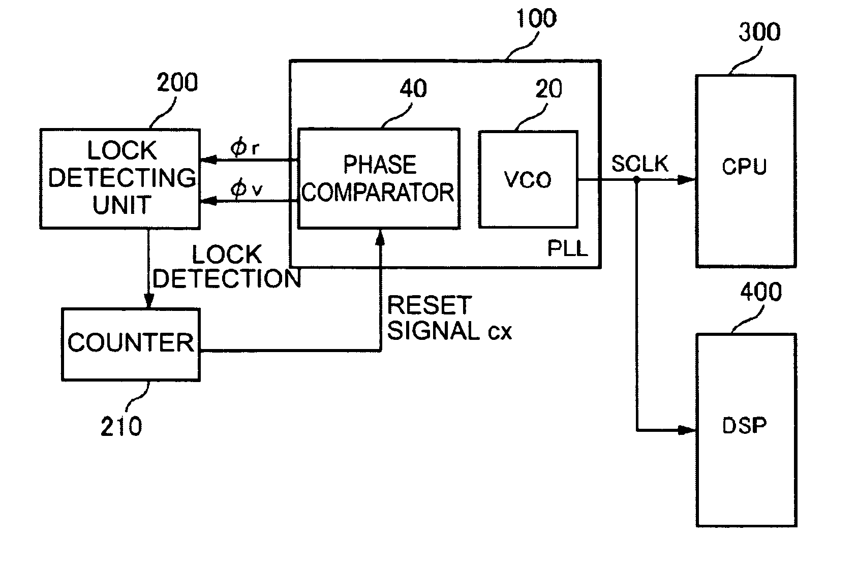
[0033]FIG. 1 is a system configuration diagram of an information processing apparatus disposed with a PLL circuit according to an embodiment of the present invention. The information processing apparatus is an electronic device disposed with the PLL circuit according to the present invention, such as a television receiver, an FM receiver, and a mobile communication device.

[0034]The information processing apparatus is disposed with a CPU 300 responsible for overall control of the system and a DSP (Digital Signal Processor) 400 for performing a predetermined digital signal process. A PLL circuit 100 is disposed to synchronize the CPU 300 and the DSP 400 and supplies the CPU 300 and the DSP 400 with a system clock signal SCLK, which is an oscillation output of a voltage controlled oscillation circuit (hereinafter, VCO) 20.

[0035]The information processing appar...


PUM


Abstract

A PLL circuit is disclosed that comprises a controlling unit that switches at a predetermined timing to enable / disable the phase difference signal supplied from the phase comparator to the low pass filter; and a resistor element that is disposed between a predetermined potential and a signal line for supplying the phase difference signal from the phase comparator to the low pass filter, when the phase difference signal is enabled, the oscillation circuit performing oscillation operation based on the voltage signal corresponding to the phase difference signal, when the phase difference signal is disabled, the low pass filter being supplied with the predetermined potential through the resistor element to allow the oscillation circuit to perform oscillation operation based on the voltage signal generated depending on the supplied predetermined potential.

Description

CROSS-REFERENCE TO RELATED APPLICATIONS[0001]This application is a National Stage Application filed under 35 U.S.C. §371 and claims the benefit of priority to International Patent Application PCT / JP2005 / 2156, filed Feb. 14, 2005, which claims priority to Japanese Patent Application No. 2004-055280, filed Feb. 27, 2004. The full contents of the international application are incorporated herein by reference.BACKGROUND OF THE INVENTION[0002]1. Technical Field[0003]The present invention relates to a PLL circuit that employs a spread spectrum technology.[0004]2. Description of the Related Art[0005]Recently, in electronic devices, speeding-up of a signal process and high-density packaging are promoted and it is an important issue to reduce EMI (Electro Magnetic Interference) noise. EMI is an electromagnetic failure causing a malfunction due to radiation noise generated by the electronic devices. The EMI noise is known to be caused mainly by a system clock signal generated by a voltage con...

Claims


Application Information

Patent Timeline
Patent Type & Authority Patents(United States)
IPC IPC(8): H03B29/00G06F1/04H03C3/00H03L7/18H03L7/093
CPCH03L7/085H03L7/18H03L7/08H03L7/093H03L7/16
Inventor KIMURA, SYUJIHASHIZUME, TAKASHI
Owner SEMICON COMPONENTS IND LLC