Phosphorescent oled having double exciton-blocking layers

a phosphorescent oled and exciton-blocking technology, which is applied in the direction of discharge tube luminescnet screens, natural mineral layered products, other domestic articles, etc., can solve the problems of not being able to fully block the triplet exciton diffusion and affecting the operation li

Active Publication Date: 2011-10-11
GLOBAL OLED TECH
View PDF102 Cites 120 Cited by
  • Summary
  • Abstract
  • Description
  • Claims
  • Application Information

AI Technical Summary

Benefits of technology

[0021]The present invention inserts a second exciton-blocking layer between the first exciton-blocking layer and the light-emitting layer to further enhance the exciton-blocking effect. It is an advantage of the present invention that the phosphorescent OLED having the second exciton-blocking layer can produce electrophosphorescence with improved quantum efficiency and operational lifetime.

Problems solved by technology

It also may not be fully block the triplet exciton diffusion from the light-emitting layer into the hole-transporting layer.
As a result, the electrophosphorescence of the phosphorescent OLED can be partially quenched and the operational lifetime can be negatively affected.

Method used


Image

  • Phosphorescent oled having double exciton-blocking layers
  • Phosphorescent oled having double exciton-blocking layers
  • Phosphorescent oled having double exciton-blocking layers

Examples


examples

[0315]The following examples are presented for a further understanding of the present invention. The reduction potential and the oxidation potential of the materials were measured using a Model CHI660 electrochemical analyzer (CH Instruments, Inc., Austin, Tex.) with the method as discussed before. During the fabrication of OLEDs, the thickness of the organic layers and the doping concentrations were controlled and measured in situ using calibrated thickness monitors built in an evaporation system (Made by Trovato Mfg., Inc., Fairport, N.Y.). The EL characteristics of all the fabricated devices were evaluated using a constant current source (KEITHLEY 2400 SourceMeter, made by Keithley Instruments, Inc., Cleveland, Ohio) and a photometer (PHOTO RESEARCH SpectraScan PR 650, made by Photo Research, Inc., Chatsworth, Calif.) at room temperature. Operational lifetime (or stability) of the devices was tested at the loom temperature and at an initial luminance of 1,000 cd / m2 by driving a c...

examples 4-6

[0341]A comparative phosphorescent OLED (Device 4) is fabricated with the same method and the same layer structure as Example 1, except that the LEL is a TPBI layer doped with 7% of Ir(ppy)3 by volume.

[0342]Device 4 is denoted as: ITO / 95 nm NPB / 20 nm TPBI:7 vol. % Ir(ppy)3 / 40 nm Bphen / 1 nm LiF / 100 nm Al. The EL performance of the device is summarized in Table 1, and its EL spectrum is shown in FIG. 6.

[0343]Another comparative phosphorescent OLED (Device 5) is fabricated with the same method and the same layer structure as Example 2, except that the LEL is a TPBI layer doped with 7% of Ir(ppy)3 by volume.

[0344]Device 5 is denoted as: ITO / 85 nm NPB / 10 nm TCTA / 20 nm TPBI:7 vol. % Ir(ppy)3 / 40 nm Bphen / 1 nm LiF / 100 nm Al. The EL performance of the device is summarized in Table 1, and its EL spectrum is shown in FIG. 6.

[0345]An inventive phosphorescent OLED (Device 6) is fabricated with the same method and the same layer structure as Example 3, except that the LEL is a TPBI layer doped wi...

examples 7-8

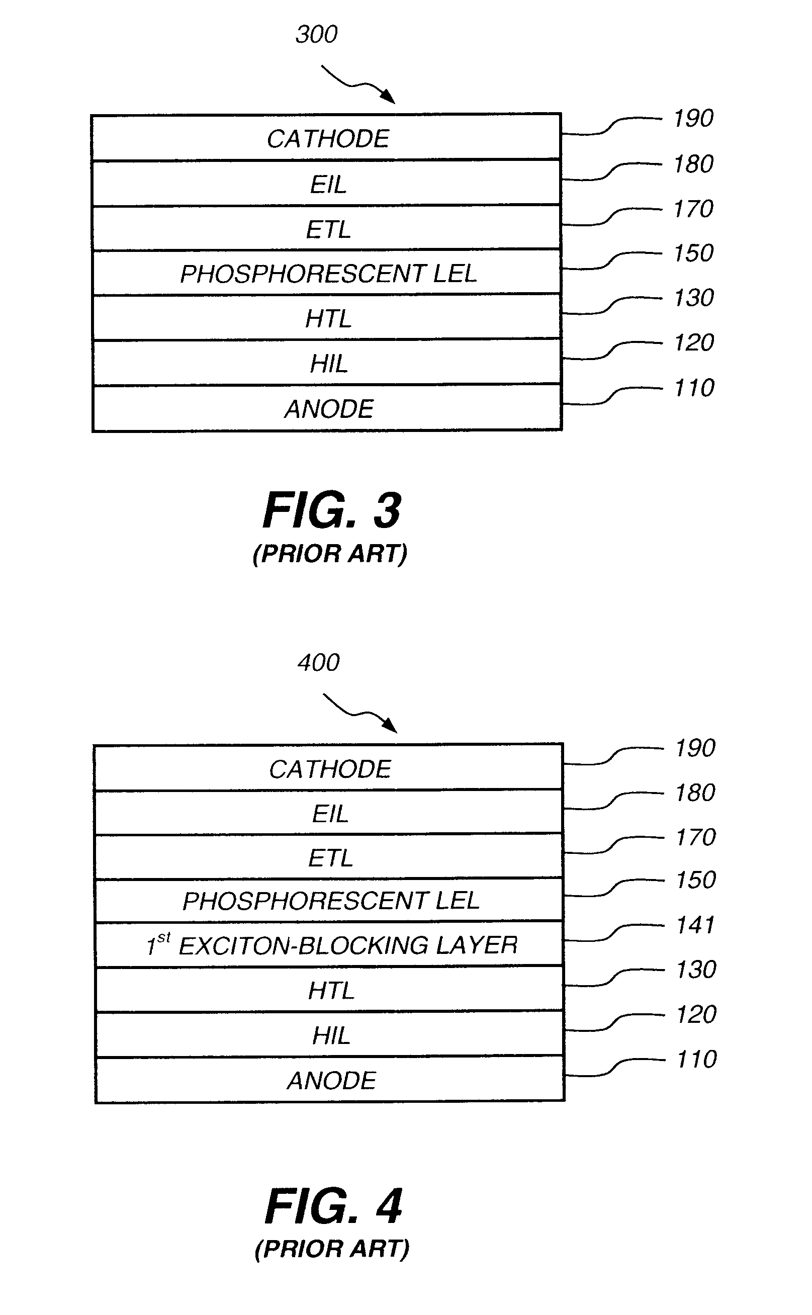
[0349]A comparative phosphorescent OLED (Device 7) is constructed in the same manner as that of Example 1. The layer structure is:

[0350]a) an HTL, 10 nm thick, including hexaazatriphenylene hexacarbonitrile (HAT-CN);

[0351]b) a HTL, 75 nm thick, including NPB;

[0352]c) a 1st EBL, 10 nm thick, including TCTA;

[0353]e) a LEL, 20 nm thick, including Bphen doped with 7% of Ir(ppy)2(cou1) by volume;

[0354]f) an ETL, 50 nm thick, including Bphen;

[0355]g) an EIL, 2 nm thick, including Formula (T-1); and

[0356]h) a cathode: approximately 100 nm thick, including Al.

[0357]Device 7 is denoted as: ITO / 10 nm HAT-CN / 75 nm NPB / 10 nm TCTA / 20 nm Bphen:7% Ir(ppy)2(cou1) / 50 nm Bphen / 2 nm (T-1) / 100 nm Al. The EL performance of the device is summarized in Table 2, and its EL spectrum is shown in FIG. 7.

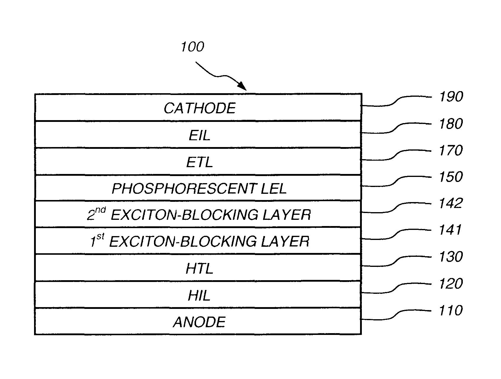
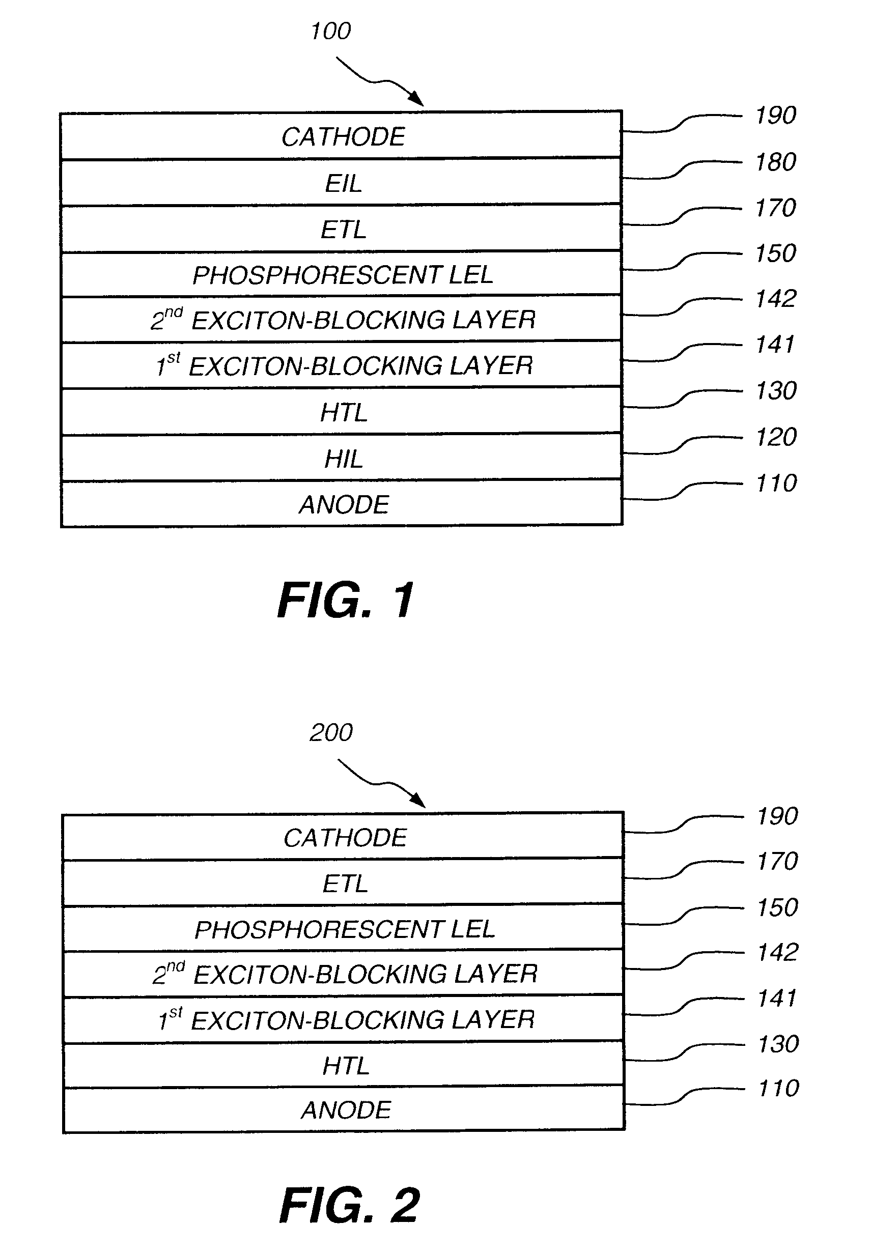
[0358]An inventive phosphorescent OLED (Device 8) is constructed in the same manner and the same layer structure as that of Example 7, except that a 2nd EXBL is inserted between the 1st EXBL and the LEL layer....


PUM

PropertyMeasurementUnit
thicknessaaaaaaaaaa
thicknessaaaaaaaaaa
thickaaaaaaaaaa

Abstract

An organic light-emitting device comprising an anode; a cathode; a hole-transporting layer disposed between the anode and the cathode; a phosphorescent light-emitting layer disposed between the hole-transporting layer and the cathode, wherein the phosphorescent light-emitting layer includes at least one host and at least one phosphorescent dopant; a first exciton-blocking layer disposed between the hole-transporting layer and the phosphorescent light-emitting layer; wherein the first exciton-blocking layer has a triplet energy greater than the triplet energy of the host in the phosphorescent light-emitting layer; and a second exciton-blocking layer disposed between the first exciton-blocking layer and the phosphorescent light-emitting layer, wherein the second exciton-blocking layer is in contact with the phosphorescent light-emitting layer, and wherein the second exciton-blocking layer has a triplet energy less than the triplet energy of the first exciton-blocking layer.

Description

CROSS REFERENCE TO RELATED APPLICATION[0001]Reference is made to commonly assigned U.S. patent application Ser. No. 11 / 749,883, filed May 17, 2007, pending, entitled “Hybrid OLED With Fluorescent and Phosphorescent Layers” by Joesph Deaton et al.; commonly assigned U.S. patent application Ser. No. 11 / 749,899, filed May 17, 2007, pending, entitled “Hybrid Fluorescent / Phosphorescent OLEDs” by Joesph Deaton et al.; and U.S. patent application Ser. No. 11 / 749,875, filed May 17, 2007 pending, entitled “Hybrid OLED Having Improved Efficiency” by Liang-Sheng Liao et al., the disclosures of which are herein incorporated by reference.FIELD OF THE INVENTION[0002]The present invention relates to organic light-emitting devices (OLEDs) or organic electroluminescent (EL) devices comprising a phosphorescent light-emitting layer and two adjacent exciton-blocking layers.BACKGROUND OF THE INVENTION[0003]Organic light-emitting devices (OLEDs) or organic electroluminescent (EL) devices have been known ...

Claims


Application Information

Patent Timeline
Patent Type & Authority Patents(United States)
IPC IPC(8): H01L51/54
CPCC09K11/06H01L51/5096H05B33/14Y10S428/917C09K2211/1011C09K2211/1014C09K2211/1029C09K2211/1044C09K2211/1048C09K2211/1059C09K2211/185C09K2211/186H01L51/0059H01L51/0085H01L51/5016C09K2211/1007H10K85/631H10K85/342H10K50/18H10K50/11H10K2101/10H10K50/00
Inventor LIAO, LIANG-SHENGREN, XIAOFANPELLOW, CYNTHIA A.TYAN, YUAN-SHENG
Owner GLOBAL OLED TECH
Why Eureka
Try Eureka