Semiconductor device and manufacturing method thereof

a semiconductor device and manufacturing method technology, applied in the direction of semiconductor devices, semiconductor/solid-state device details, electrical apparatus, etc., can solve the problems of increasing the manufacturing and increasing the cost of the semiconductor device b>100/b>, so as to suppress the occurrence of dielectric loss

Active Publication Date: 2011-10-11
SHINKO ELECTRIC IND CO LTD
View PDF3 Cites 4 Cited by
  • Summary
  • Abstract
  • Description
  • Claims
  • Application Information

AI Technical Summary

Benefits of technology

[0012]Exemplary embodiments of the present invention provide a semiconductor device capable of suppressing occurrence of a dielectric loss if the device is miniaturized and a manufacturing method of the semiconductor device.
[0026]According to the invention, the device can be miniaturized. The ground layer and the passive layer are provided through the inorganic insulating layer having a small dielectric loss as compared with a resin insulating layer, so that delay occurrence of signal transfer can be suppressed and therefore the antenna characteristic can be improved.

Problems solved by technology

However, the semiconductor device 100 described above involves a problem of an increase in the manufacturing cost of the semiconductor device 100 because the chip antenna 104 is expensive.
To use the chip antenna 104, the matching component 105 for adjusting an impedance needs to be provided and thus the area of the board 101 grows, the cost of the semiconductor device 100 increases, and the semiconductor device 100 cannot be miniaturized; this is a problem.
Inevitably, an insulating material needs to be provided between the antenna and the semiconductor chip, however, since the semiconductor chip and the antenna pattern are isolated using an insulating resin in the related art, the dielectric loss is large because of the insulating resin and any desired antenna characteristic cannot be provided; this is a problem.
Particularly, for a millimeter waveband antenna, the dielectric loss becomes a large problem.

Method used


Image

  • Semiconductor device and manufacturing method thereof
  • Semiconductor device and manufacturing method thereof
  • Semiconductor device and manufacturing method thereof

Examples


first embodiment

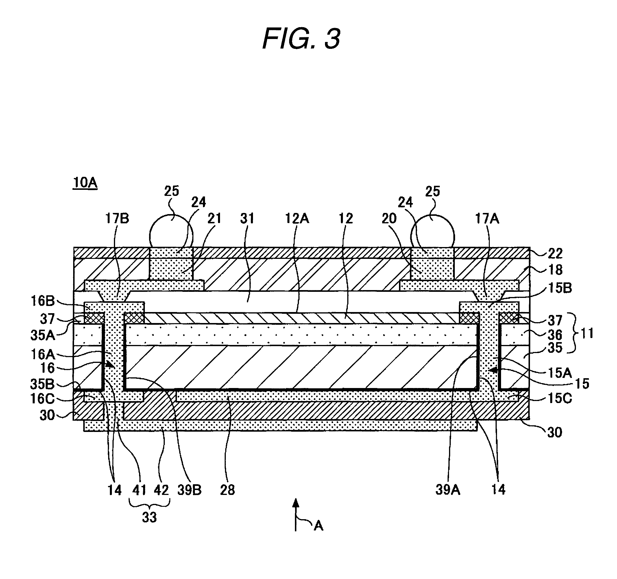
[0057]FIG. 3 is a sectional view of a semiconductor device according to the invention. A semiconductor device 10A is electrically connected to a mount board (not shown) such as a mother board, for example, through external connection terminals 25. In the description of the embodiment, the case where a patch antenna 33 is used as a passive element is taken as an example.

[0058]The semiconductor device 10A has a semiconductor chip 11, a protective film 12, an insulating film 14, a solder resist 22, through electrodes 15 and 16, re-wirings 17A and 17B, a seal resin 18, posts and 21, a diffusion prevention film 24, the above-mentioned external connection terminals 25, a ground layer 28, an inorganic insulating layer 30, and the above-mentioned patch antenna 33 as a passive element.

[0059]The semiconductor chip 11 has a semiconductor substrate 35, an element formation layer 36, electrode pads 37, through holes 39A and 39B passing through the electrode pads 37, and the like. The semiconduct...

fifth embodiment

[0114]Further, in place of antenna, a shield layer may be applied as the passive layer in a semiconductor device 10E according to the invention shown in FIGS. 24A and 24B. A ground layer 128 is formed of Cu and is provided on the whole second face 35B of the semiconductor substrate 35. The ground layer 128 is electrically connected to a connection part 15C of the through electrode 15 which is electrically connected to a ground line of a semiconductor element. The ground layer 128 is also electrically connected to a connection part 116C of a through electrode 116 which has a connection part 116B and a through part 116A and is electrically connected to a ground line of the semiconductor element. A shield layer 133 is made of Ni and is provided on the whole second face 35B of the semiconductor substrate 35 through an inorganic insulating layer 30. The shield layer 133 is electrically connected to the ground layer 128 through GND terminals 105 and 106. According to the semiconductor dev...


PUM


Abstract

A semiconductor device has a semiconductor chip and through electrodes formed passing through the semiconductor chip. A ground layer connected to the through electrode and a patch antenna connected to the through electrode are provided through an inorganic insulating layer formed of SiO2 or SiN on a second face opposite to a first face (main face) of the semiconductor chip.

Description

TECHNICAL FIELD[0001]The present disclosure relates to a semiconductor device and a manufacturing method thereof and in particular to a semiconductor device including a passive element and a manufacturing method of the semiconductor device.RELATED ART[0002]Some semiconductor devices include an antenna as a passive element. Such a semiconductor device includes a board and a CPU semiconductor chip, an RF device, etc., provided on the board; it is used, for example, as a wireless module. A chip antenna, an antenna pattern, etc., is use as the antenna.[0003]FIG. 1 is a sectional view of a semiconductor device in a related art including a chip antenna. As shown in the figure, a semiconductor device 100 has a board 101, a CPU semiconductor chip 102, an RF device 103, a chip antenna 104, and a matching component 105.[0004]The board 101 is formed with a wiring pattern not shown. The CPU semiconductor chip 102, the RF device 103, the chip antenna 104, and the matching component 105 are provi...

Claims


Application Information

Patent Timeline
Patent Type & Authority Patents(United States)
IPC IPC(8): H01L27/08
CPCH01L21/76898H01L24/03H01L24/94H01L2924/0002H01L2224/05571H01L2224/02372H01L2224/05024H01L2224/05569H01L24/05H01L24/11H01L24/13H01L2224/0401H01L2224/94H01L2924/01004H01L2924/01013H01L2924/01014H01L2924/01022H01L2924/01029H01L2924/01047H01L2924/01051H01L2924/01078H01L2924/01079H01L2924/014H01L2924/3011H01L2924/3025H01L2924/01005H01L2924/01006H01L2924/01024H01L2924/01033H01L2924/01075H01L2224/11H01L2924/00012H01L2224/05552H01L23/48H01L23/485
Inventor FUJII, TOMOHARU
Owner SHINKO ELECTRIC IND CO LTD
Why Eureka
Try Eureka