

Signal processing device, image sensing system, and signal processing method
- Summary
- Abstract
- Description
- Claims
- Application Information
AI Technical Summary
Benefits of technology
Problems solved by technology
Method used
Image

Examples
first embodiment
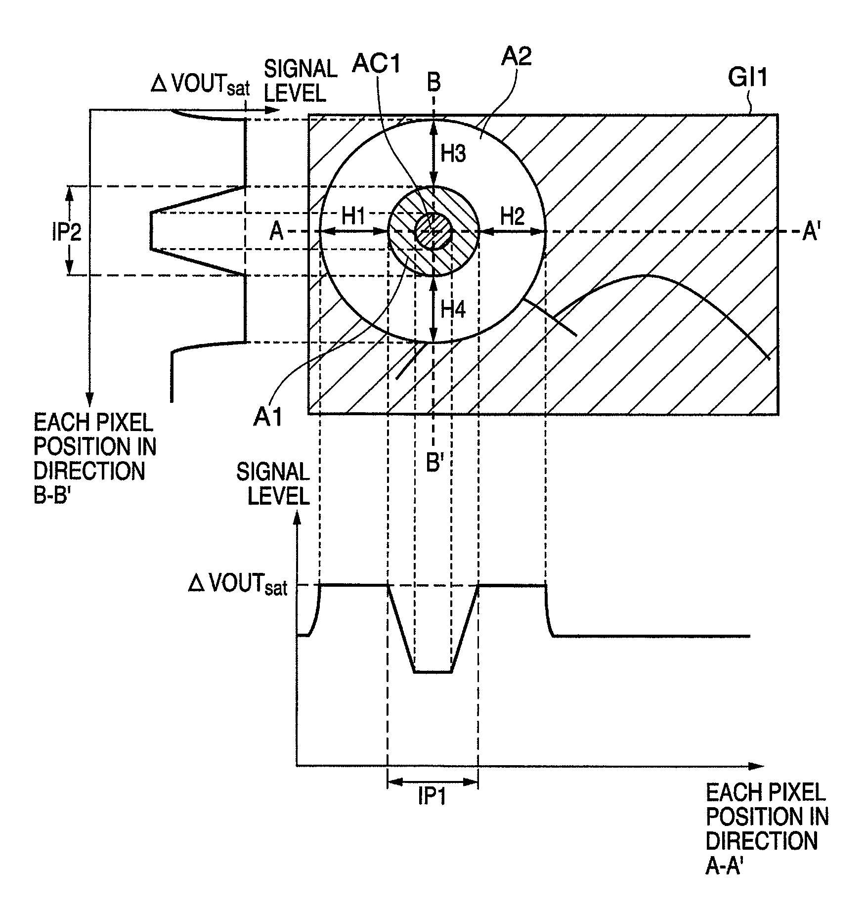
An image sensing system according to the present invention will be described. The image sensing system is applicable not only to a so-called digital camera, digital video camera, and the like, but also to contact type line sensors such as a scanner and copying machine.
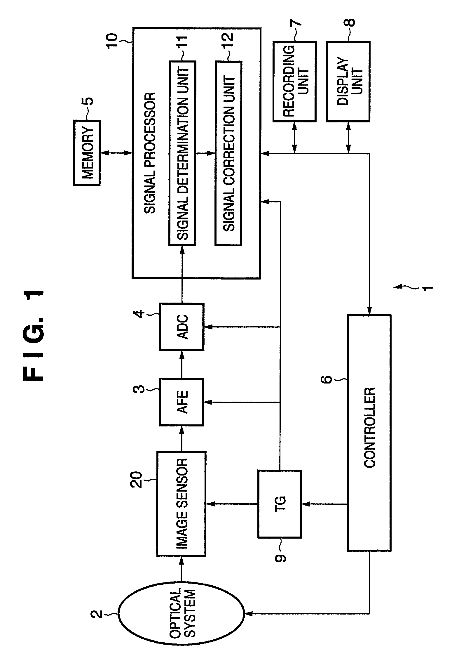
The schematic configuration and schematic operation of the image sensing system according to the first embodiment of the present invention will be described with reference to FIG. 1. FIG. 1 is a block diagram of the configuration of the image sensing system according to the first embodiment of the present invention.
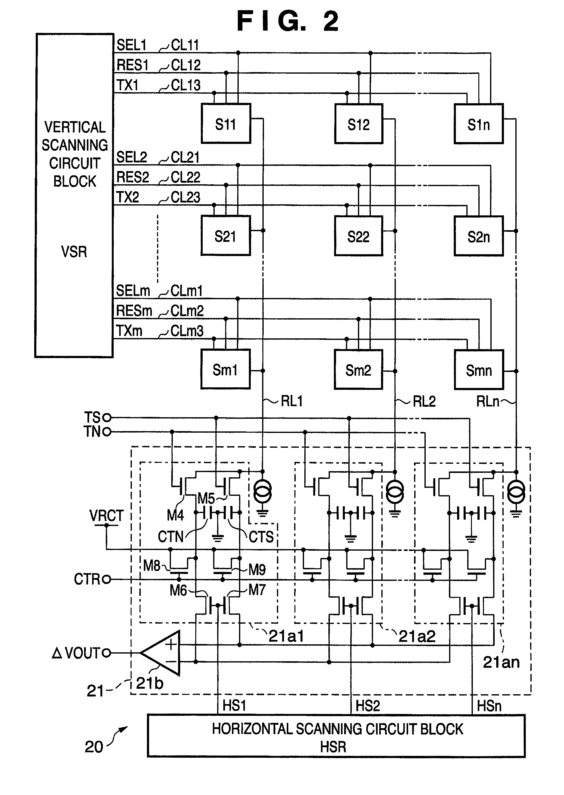
An image sensing system 1 comprises an optical system 2, image sensor 20, AFE (Analog Front End) 3, ADC (Analog Digital Converter) 4, signal processor (signal processing device) 10, memory 5, recording unit 7, display unit 8, controller 6, and TG (Timing Generator) 9.
The optical system 2 is interposed between an object (not shown) and the image sensor 20, and forms an optical image of the object on the image...
PUM
 Abstract
Description
Claims
Application Information