Organic light-emitting device, and methods of forming the same and electronic devices having the same

a light-emitting device and organic technology, applied in the direction of discharge tube luminescnet screens, discharge tube/lamp details, electric discharge lamps, etc., can solve the problems of prone to damage, broken, and type of organic light-emitting devices, so as to facilitate the shrinkage of display panels, increase the effective light-emitting area, and avoid complicated process flow

Active Publication Date: 2011-11-08
INNOLUX CORP
View PDF8 Cites 2 Cited by
  • Summary
  • Abstract
  • Description
  • Claims
  • Application Information

AI Technical Summary

Benefits of technology

[0008]Another aspect of the present invention is to provide an organic light-emitting device with increased effective light-emitting area to facilitate the shrinkage of the display panel.
[0009]Further aspect of the present invention is to provide a method of forming an organic light-emitting device with an electrode contact in the peripheral circuit area compatible with current processes without complicating the process flow.

Problems solved by technology

However, the cathode layer 11 in the peripheral circuit area 11 is prone to damage (i.e. broken) because the aspect ratio of the contact hole 16 is too high and the cathode layer 11 is too thin. FIG. 1B is a cross-sectional view of another conventional organic light-emitting device 100 in the related art.
However, this kind of organic light-emitting device also has some drawbacks.
For example, every pixel needs to sacrifice certain areas to serve as contact regions of the cathode electrode 114 so that the available light-emitting area is decreased, and the resolution and the possible shrinkage of the display are restricted.

Method used


Image

  • Organic light-emitting device, and methods of forming the same and electronic devices having the same
  • Organic light-emitting device, and methods of forming the same and electronic devices having the same
  • Organic light-emitting device, and methods of forming the same and electronic devices having the same

Examples


first embodiment

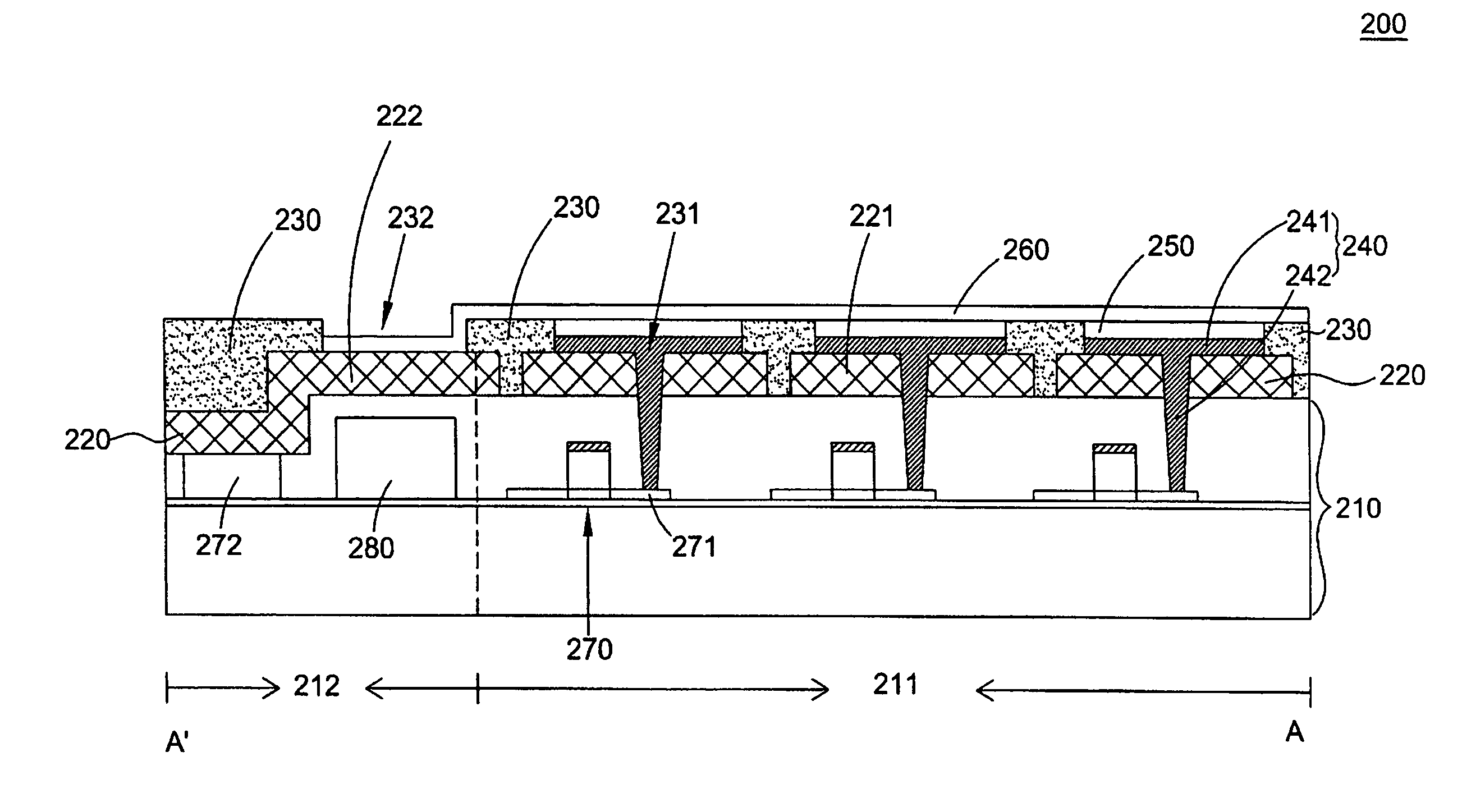
[0020]Referring to FIG. 2, a cross-sectional view of an organic-light emitting device 200 is shown in accordance with the present invention. In the embodiment, the organic-light emitting device 200 is illustrated with a top emission organic light-emitting device. As shown in FIG. 2, the organic light-emitting device 200 includes a substrate 210 having a pixel area 211 and a peripheral circuit area 212. For example, the pixel area 211 is generally the center region of the display panel for displaying information, and the peripheral circuit area 212 is generally the peripheral region of the display panel used for control / driving circuits. A transistor 270 including a device electrode layer 271 (such as source / drain regions) is formed in the pixel area 211 of the substrate 210. It is noted that the transistor 270 formed in the pixel area 271 is used to control the pixels. Besides, a signal electrode layer 272 and a peripheral circuit system 280 (including the transistors for the periph...

third embodiment

[0031]FIG. 5 is a cross-sectional view of an organic-light emitting device 500 in accordance with the present invention. As shown in FIG. 5, compared with the organic light-emitting device 200 and 400, the pixel definition layer 530 in the pixel area 211 of the organic-light emitting device 500 is a rectangular shape instead of a T shape as illustrated for the pixel definition layer 230 in the pixel area in the above-mentioned embodiments. Thus, in this embodiment, the first reflective part 221 is adjacent to the pixel definition layer 530 in the plurality of pixel openings 231. However, when the pixel definition layer is a T shape, a portion of the first reflective part 221 may be sandwiched between the pixel definition layer 230 and the substrate 210 (as shown in FIG. 2), and / or the first part 241 of the first electrode layer 240 may be sandwiched between the pixel definition layer 230 and the first electrode layer 240 (not shown). In general, the structure of the pixel definition...

fourth embodiment

[0032]FIG. 6 is a schematic diagram illustrating an electronic device60 in accordance with the present invention. In FIG. 6, the electronic device 60 includes an image display system 62, which includes an organic light-emitting device and an input unit 64. For example, the electronic device 60 may be a cellular phone, a digital camera, a personal digital assistant (PDA), a laptop computer, a desktop computer, a television, an automobile display, an aircraft display, a global positioning system (GPS), or a portable DVD player, etc. The organic light-emitting device may be an organic light-emitting device 200, 400, or 500 disclosed in the foregoing embodiments or the likes. In this embodiment, the organic light-emitting device 200 is illustrated. Moreover, the input unit 64 is coupled to the organic light-emitting device 200 and configured to providing a signal for controlling the organic light-emitting device 200 to display image.


PUM


Abstract

An organic light-emitting device and methods of forming the same are provided. The organic light-emitting device includes: a substrate having a pixel area and a peripheral circuit area; a reflective layer on the substrate, the reflective layer having a first reflective part in the pixel area and a second reflective part in the peripheral circuit area; a first electrode layer having a first part on the first reflective part; a pixel definition layer on the substrate, the pixel definition layer forming a plurality of pixel openings to expose a portion of the first part of the first electrode layer and at least one electrode contact hole to expose the second reflective part; an organic light-emitting layer on the first electrode layer; and a second electrode layer on the organic light-emitting layer, the second electrode layer extending to the peripheral circuit area to electrically couple with the exposed area of the second reflective part.

Description

CROSS REFERENCE TO RELATED APPLICATIONS[0001]This application claims the right of priority based on Taiwan Patent Application No. 096124468 entitled “organic light emitting device, and methods of forming the same and electronic devices having the same,” filed on Jul. 5, 2007, which is incorporated herein by reference and assigned to the assignee herein.FIELD OF THE INVENTION[0002]This invention relates to an organic light-emitting device, and more particularly, to an organic light-emitting device for resolving the broken electrode issue and increasing the light-emitting area, and methods of forming the same and an electronic device having the same.BACKGROUND OF THE INVENTION[0003]In recent years, the organic light-emitting displays are widely used in many consumer electronic products due to those advantageous characteristics, such as self-luminescence, wide viewing angle, high response speed, high color saturation and flexile panels. Generally, an organic light emitting display incl...

Claims


Application Information

Patent Timeline
Patent Type & Authority Patents(United States)
IPC IPC(8): H01J1/62H01J63/04
CPCH01L27/3246H01L27/3276H01L51/5271H05B33/06H05B33/22H05B33/28H10K59/122H10K50/856H10K59/1315H10K59/8052H10K59/131
Inventor CHAN, CHUAN-YIPENG, DU-ZEN
Owner INNOLUX CORP
Why Eureka
Try Eureka