
System and method for providing error correction and detection in a memory system

a memory system and error correction technology, applied in error detection/correction, instruments, coding, etc., can solve the problems of unfavorable data reading, fast zero error rate due, dramatic increase in failure rate, etc., to reduce the probability of uncorrectable and undetectable errors in the memory system, facilitate data reading, and facilitate error detection and correction.

Active Publication Date: 2011-11-08
GLOBALFOUNDRIES U S INC
View PDF4 Cites 3 Cited by
  • Summary
  • Abstract
  • Description
  • Claims
  • Application Information

AI Technical Summary

Benefits of technology

This approach maximizes error coverage and reliability in high-speed memory systems by ensuring that errors are correctable and detectable, preventing system failures and data corruption, while minimizing pincount overhead and maintaining performance.

Problems solved by technology

Bit error rates due solely to I / O transfer failure (e.g. the inability to pass data between the memory device and the device to which the memory device is connected) was almost zero in a properly designed and tuned (e.g. proper driver strengths, terminations, wiring topologies, etc) system.
With the increased data rates that are expected with emerging technologies (such as DDR4 and beyond), the very high data rates are expected to result in a dramatic increase in failure rates due to the inability of the memory device to accurately communicate with the device(s) (e.g., a memory interface device or “MID”) to which it is attached, given the reduced timing margins present at the high data rates.
These new errors will be caused by several factors such as clock jitter, inter symbol interference (ISI), cross-talk (between adjacent and otherwise nearby lines), etc.
Of those listed, clock jitter is expected to be a major component in the increased failure rates, comprising almost half of the total failure rate.
For this reason, the existence of a communication interface fault, at a given point in time in a high speed memory interface, suggests that there is a high probability that one or more other pins that are simultaneously switching may also have an error at the same time.
Further compounding the situation is the likelihood that the number of errors (e.g. including at least three or more independent errors) will exceed the capability of contemporary / available ECC schemes which are developed to detect random errors that have almost zero correlation between different pins or different devices.
One method of addressing this concern is through the use of a cyclic redundancy check (CRC) coding, however, this solution requires additional pins (adding cost overhead) and may dramatically affect overall memory performance due to the need to initiate one or more re-try operations until a successful transfer is completed.
CRC results in only error detection.

Method used


Image

  • System and method for providing error correction and detection in a memory system
  • System and method for providing error correction and detection in a memory system
  • System and method for providing error correction and detection in a memory system

Examples


Embodiment Construction

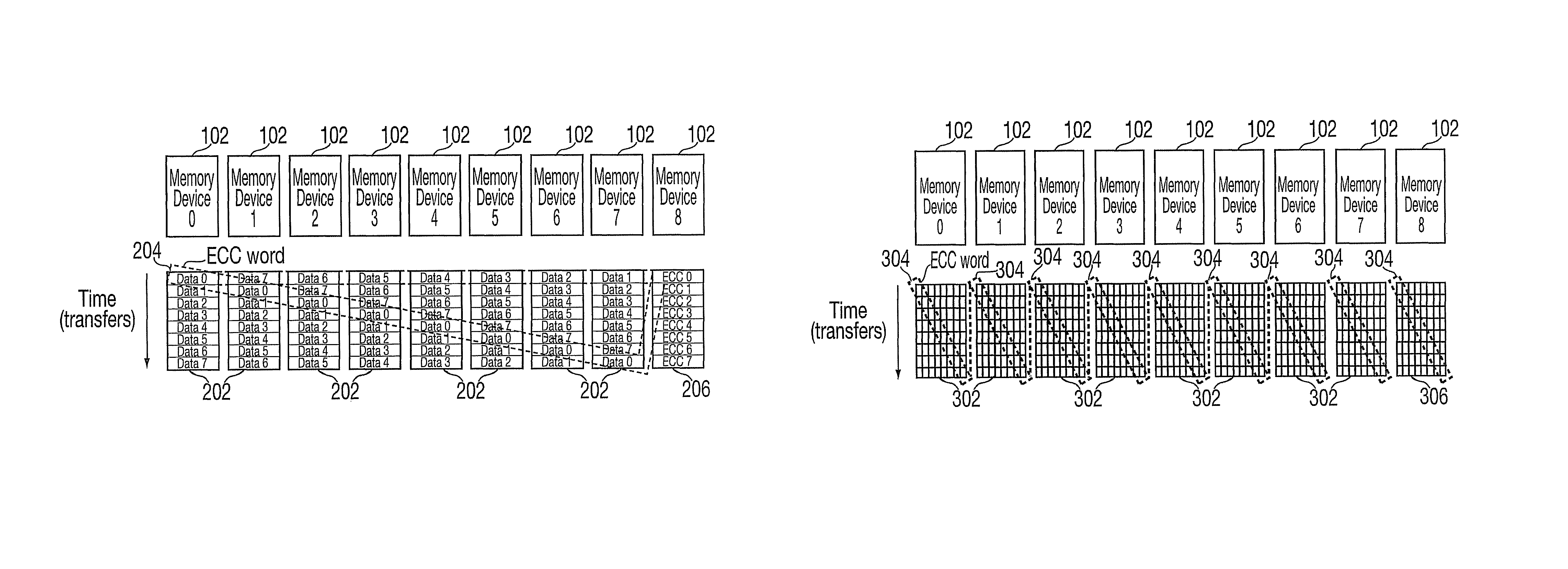
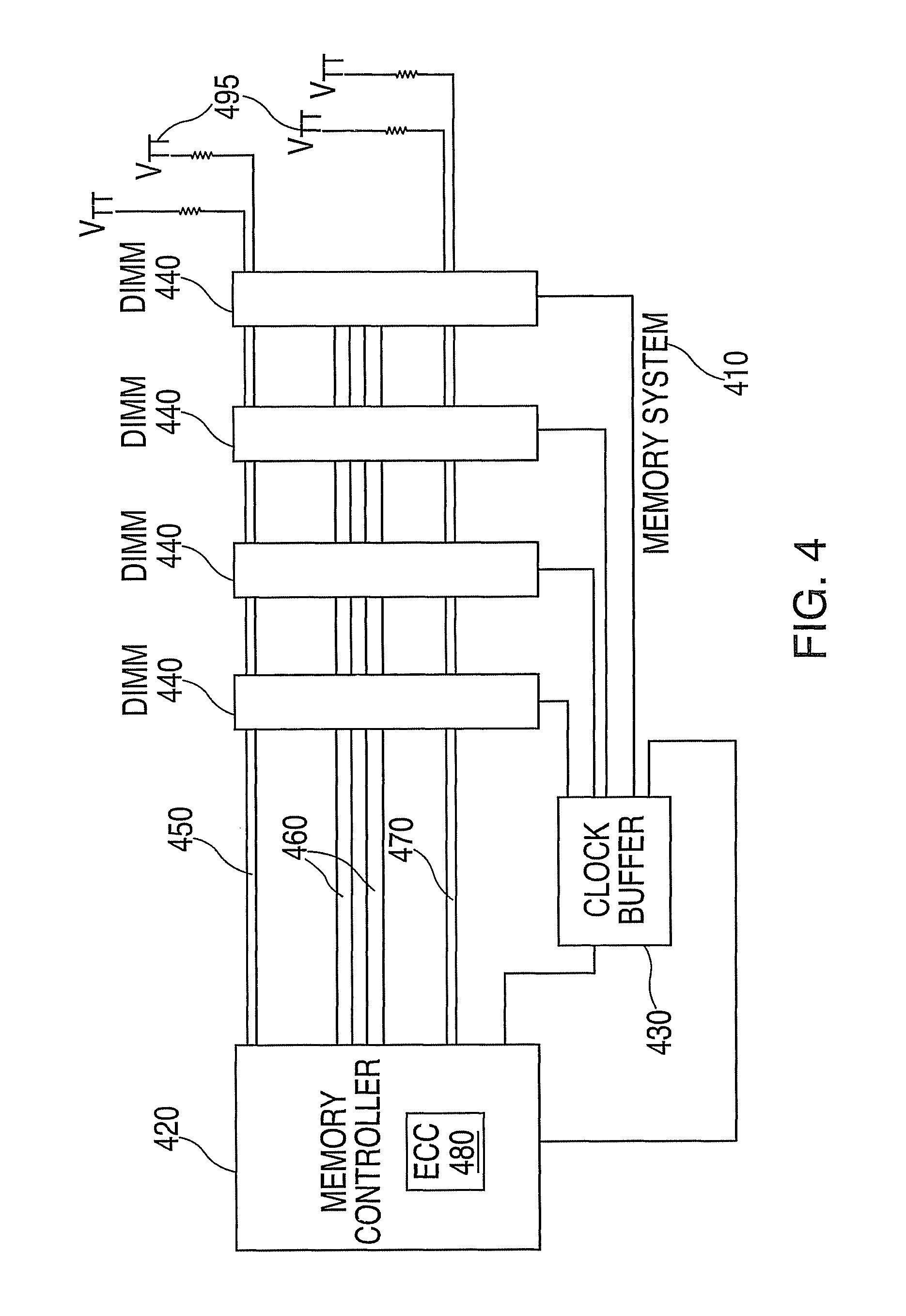
[0019]The invention relates to error correction codes (ECCs) and a manner of mapping an ECC in a high-speed memory system comprised of multiple memory devices.

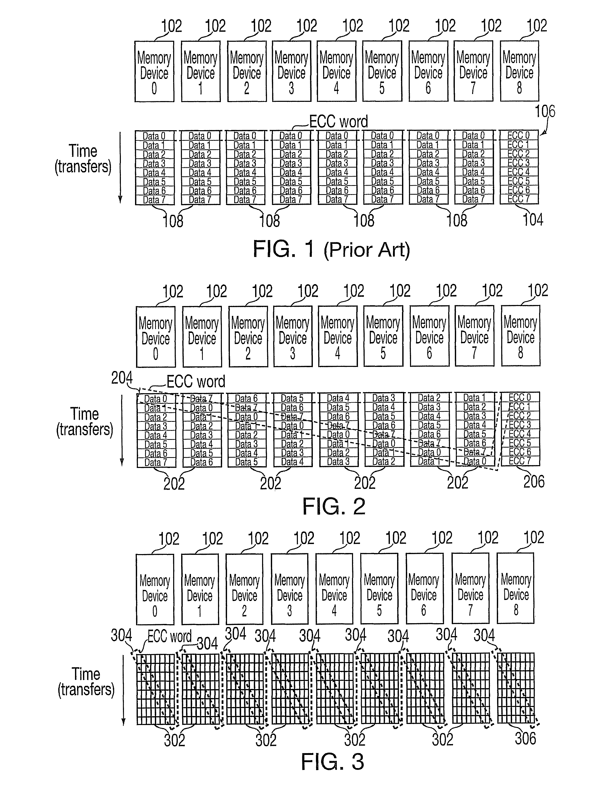
[0020]FIG. 1 is an example of a conventional ECC word mapping, where the ECC is applied and calculated for data in the same transfer (beat). FIG. 1 depicts nine memory devices 102, a data access with a burst of eight including data bits 108 and ECC bits 104, and an ECC code word 106 that spans a single transfer. If there is a strong correlation between bit errors across different devices during the same transfer (as described earlier), this method will result in a high likelihood that the available ECC will be unable to correct, or even detect (due to the limited strength of the ECC in detecting multiple errors) the existence of the multiple errors, which may result in uncorrectable or even undetectable errors. At a minimum this results in a system failure, at a maximum this results in data corruption that is not detected by t...


PUM


Abstract

A system and method for providing error correction and detection in a memory system. The memory system includes a plurality of memory devices, and error detection and correction logic. The error detection and correction logic includes instructions for generating an error correction code (ECC) word that includes bits from two more of the memory devices and from different memory device transfers.

Description

BACKGROUND OF THE INVENTION[0001]This invention relates generally to computer memory, and more particularly to providing error correction and detection in a memory system.[0002]Contemporary high performance computing main memory systems utilize error correction codes (ECCs) to detect and correct occasional, random bit errors.[0003]Historically, for memory devices up through double data rate three (DDR3), most memory errors in a memory subsystem or system could be classified as being related to one or more of memory cell faults (generally affecting a single bit), memory core errors (e.g. word line or bit line errors affecting multiple bits, etc.), I / O errors (affecting one I / O of a device), “chip kills” (affecting all I / Os of a device) or other faults due to interconnect or interface device faults, etc. Bit error rates due solely to I / O transfer failure (e.g. the inability to pass data between the memory device and the device to which the memory device is connected) was almost zero i...

Claims


Application Information

Patent Timeline
Patent Type & Authority Patents(United States)
IPC IPC(8): H03M13/00
CPCG06F11/1012G11C2029/0411
Inventor KIM, KYU-HYOUNCOTEUS, PAUL W.LASTRAS-MONTANO, LUIS A.
Owner GLOBALFOUNDRIES U S INC
Learn More