Method for design and manufacture of a reticle using a two-dimensional dosage map and charged particle beam lithography

a technology of charged particle beam and dosage map, applied in the field of lithography, can solve the problems of increasing the total time required for the charge particle beam system, the resulting photomask, and increasing the cost of the reticl

Active Publication Date: 2011-11-22
D2S
View PDF25 Cites 25 Cited by
  • Summary
  • Abstract
  • Description
  • Claims
  • Application Information

AI Technical Summary

Problems solved by technology

Multi-pass writing has a disadvantage of increasing the total time required for the charged particle beam system to form the pattern on the reticle.
This extra time increases the cost of the reticles and the resulting photomasks.
At present, no available CP charged particle beam system is suitable for use in making photomasks.
Because of the assumed normal dosage, the fracturing programs that assign VSB shots conventionally do not output dosage information.
The cost of charged particle beam lithography is directly related to the time required to expose a pattern on a surface, such as a reticle or wafer.
When these techniques are used, calculation of the pattern that will be registered by the resist is more complicated.
Charged particle beam simulation, which may include simulation of various charged particle beam writing and resist effects, is a compute-intensive process, however.
It is impractical to simulate the pattern for an entire integrated circuit, and then to re-simulate the pattern every time a proposed charged particle beam shot is changed.

Method used


Image

  • Method for design and manufacture of a reticle using a two-dimensional dosage map and charged particle beam lithography
  • Method for design and manufacture of a reticle using a two-dimensional dosage map and charged particle beam lithography
  • Method for design and manufacture of a reticle using a two-dimensional dosage map and charged particle beam lithography

Examples


Embodiment Construction

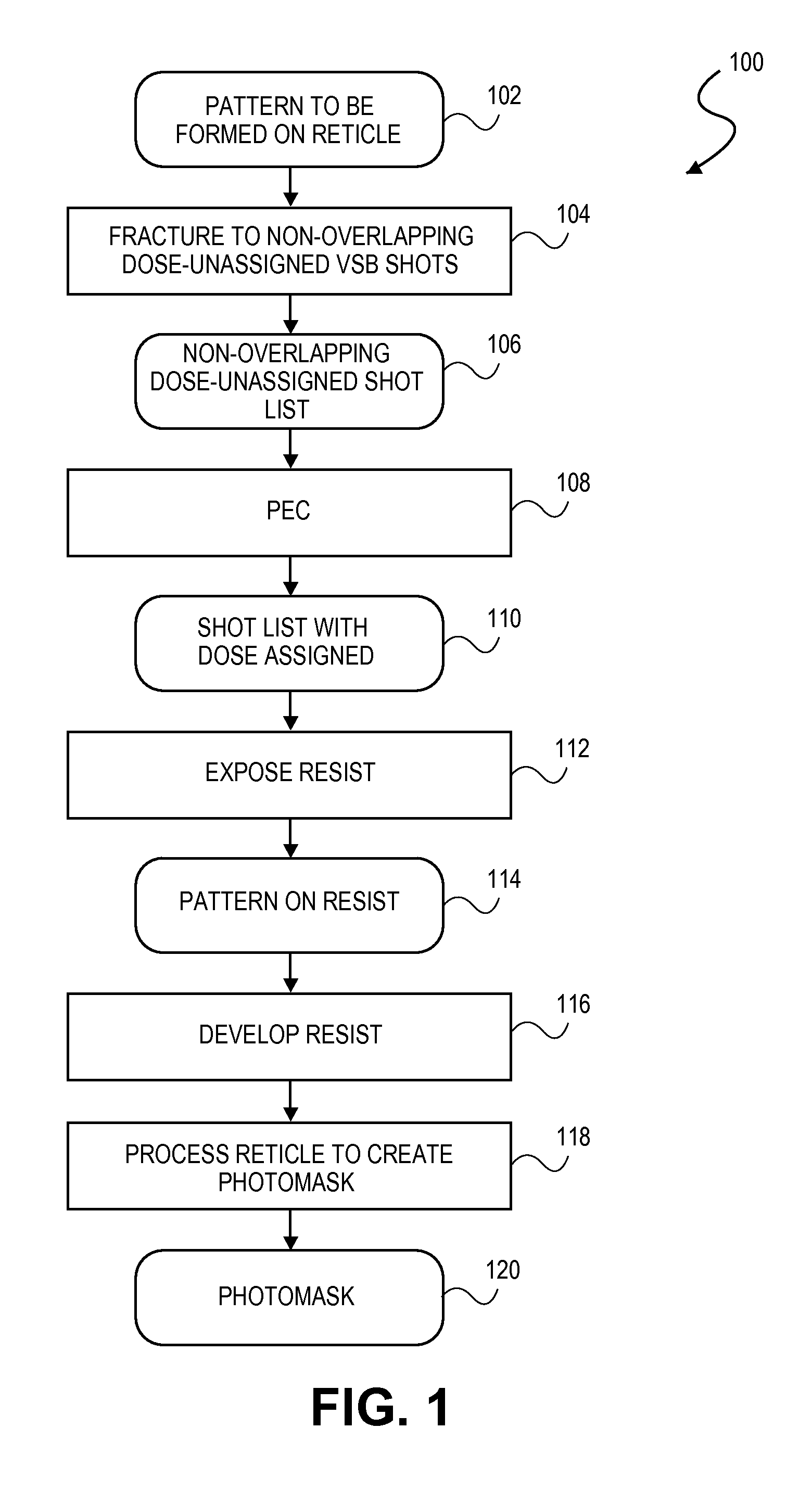
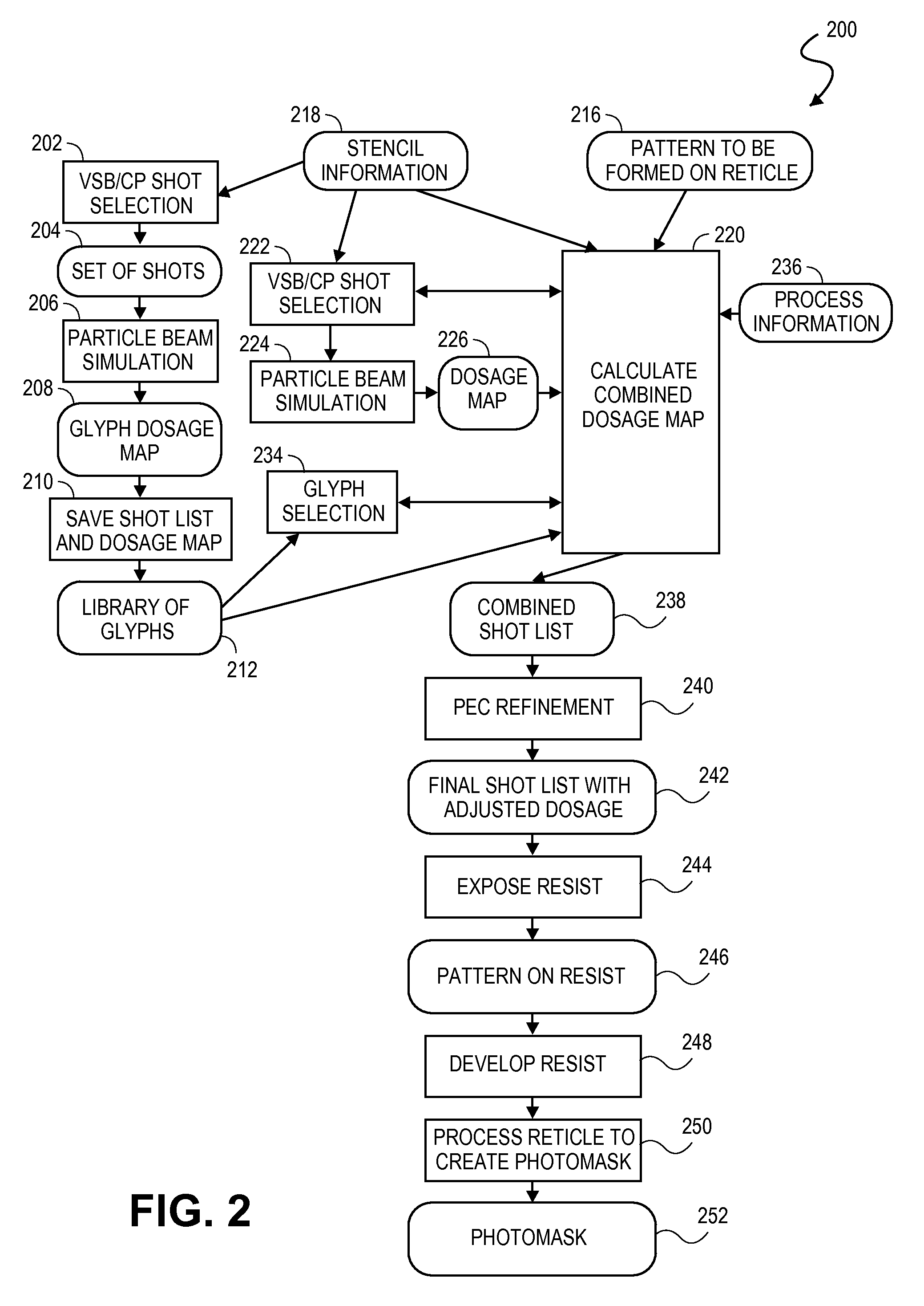
FIG. 1 illustrates a conceptual flow diagram 100 of a conventional method for making a photomask. The input to the process is a computer representation 102 of a desired pattern that is to be formed on a reticle from which the photomask can be manufactured. In step 104 the pattern is fractured into a set of non-overlapping shapes, such as rectangles and triangles, for exposure using a VSB charged particle beam system. The result of step 104 is a shot list 106, in which the shots are non-overlapping. All shots are assumed to have a normal dosage, and no dosage information is contained in shot list 106. In step 108 proximity effect correction (PEC) is performed, which assigns a dosage to each shot in the shot list, and which may also slightly adjust the placement of the shots. Step 108 may also include other corrections which perform dosage adjustments. The output of step 108 is a final shot list 110 which includes dosage information. In step 112 a charged particle beam system uses the...


PUM

PropertyMeasurementUnit
diameteraaaaaaaaaa
diameteraaaaaaaaaa
sizesaaaaaaaaaa

Abstract

In the field of semiconductor device production, a method for manufacturing a surface using two-dimensional dosage maps is disclosed. A set of charged particle beam shots for creating an image on the surface is determined by combining dosage information such as dosage maps for a plurality of shots into the dosage map for the surface. A similar method is disclosed for fracturing or mask data preparation of a reticle image.

Description

BACKGROUND OF THE DISCLOSUREThe present disclosure is related to lithography, and more particularly to the design and manufacture of a surface which may be a reticle, a wafer, or any other surface, using charged particle beam lithography.In the production or manufacturing of semiconductor devices, such as integrated circuits, optical lithography may be used to fabricate the semiconductor devices. Optical lithography is a printing process in which a lithographic mask or photomask manufactured from a reticle is used to transfer patterns to a substrate such as a semiconductor or silicon wafer to create the integrated circuit. Other substrates could include flat panel displays or even other reticles. Also, extreme ultraviolet (EUV) or X-ray lithography are considered types of optical lithography. The reticle or multiple reticles may contain a circuit pattern corresponding to an individual layer of the integrated circuit and this pattern can be imaged onto a certain area on the substrate...

Claims


Application Information

Patent Timeline
Patent Type & Authority Patents(United States)
IPC IPC(8): G03F9/00
CPCH01J37/3174G06F17/5009B82Y40/00G03F7/2063Y10S430/143G03F1/14G03F7/20B82Y10/00G03F1/78G06F30/20
Inventor ZABLE, HAROLD ROBERTFUJIMURA, AKIRA
Owner D2S
Why Eureka
Try Eureka