Imaging apparatus and radiation imaging apparatus

a radiation imaging and imaging apparatus technology, applied in the direction of x/gamma/cosmic radiation measurement, instruments, radioation controlled devices, etc., can solve the problems of deterioration of characteristics and fluctuation in sensitivity, and achieve the effect of increasing the electricity conduction time of the transfer switch 102, increasing the resistance of the gate wiring 105, and increasing the sensitivity

Inactive Publication Date: 2011-11-29
CANON KK
View PDF21 Cites 24 Cited by
  • Summary
  • Abstract
  • Description
  • Claims
  • Application Information

AI Technical Summary

Benefits of technology

[0014]From the above, it will be clear that an object of the present invention is to prevent deterioration of characteristics in the imaging apparatus and radiation imaging apparatus having small pixel pitches and capable of easily identifying a defective pixel in the defect inspection process.
[0018]According to the present invention, it is easy to identify defective pixels in a defect inspection process. Further, it is possible to prevent deterioration of the characteristics of the apparatus even in imaging apparatus and radiation imaging apparatus having small pixel pitches.

Problems solved by technology

As a result, a parasitic capacitance between each wiring and the conversion element 101 fluctuates within the radio imaging sensor panel, and this causes a fluctuation in sensitivity.
Thus, in either case, deterioration of characteristics is likely to be caused.

Method used


Image

  • Imaging apparatus and radiation imaging apparatus
  • Imaging apparatus and radiation imaging apparatus
  • Imaging apparatus and radiation imaging apparatus

Examples


first embodiment

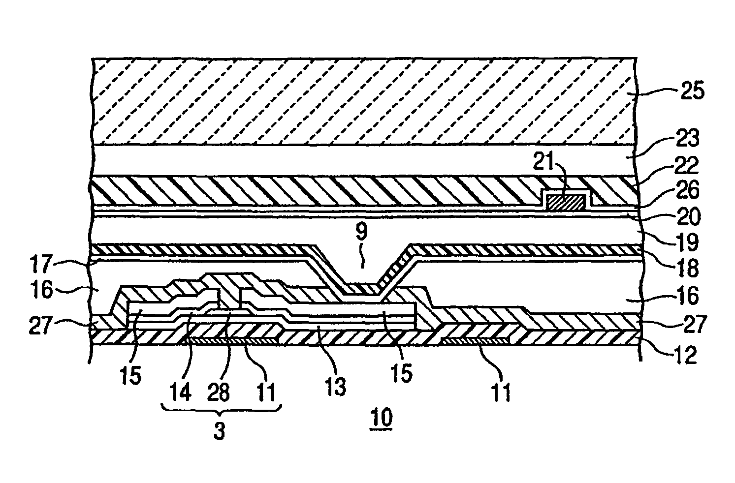
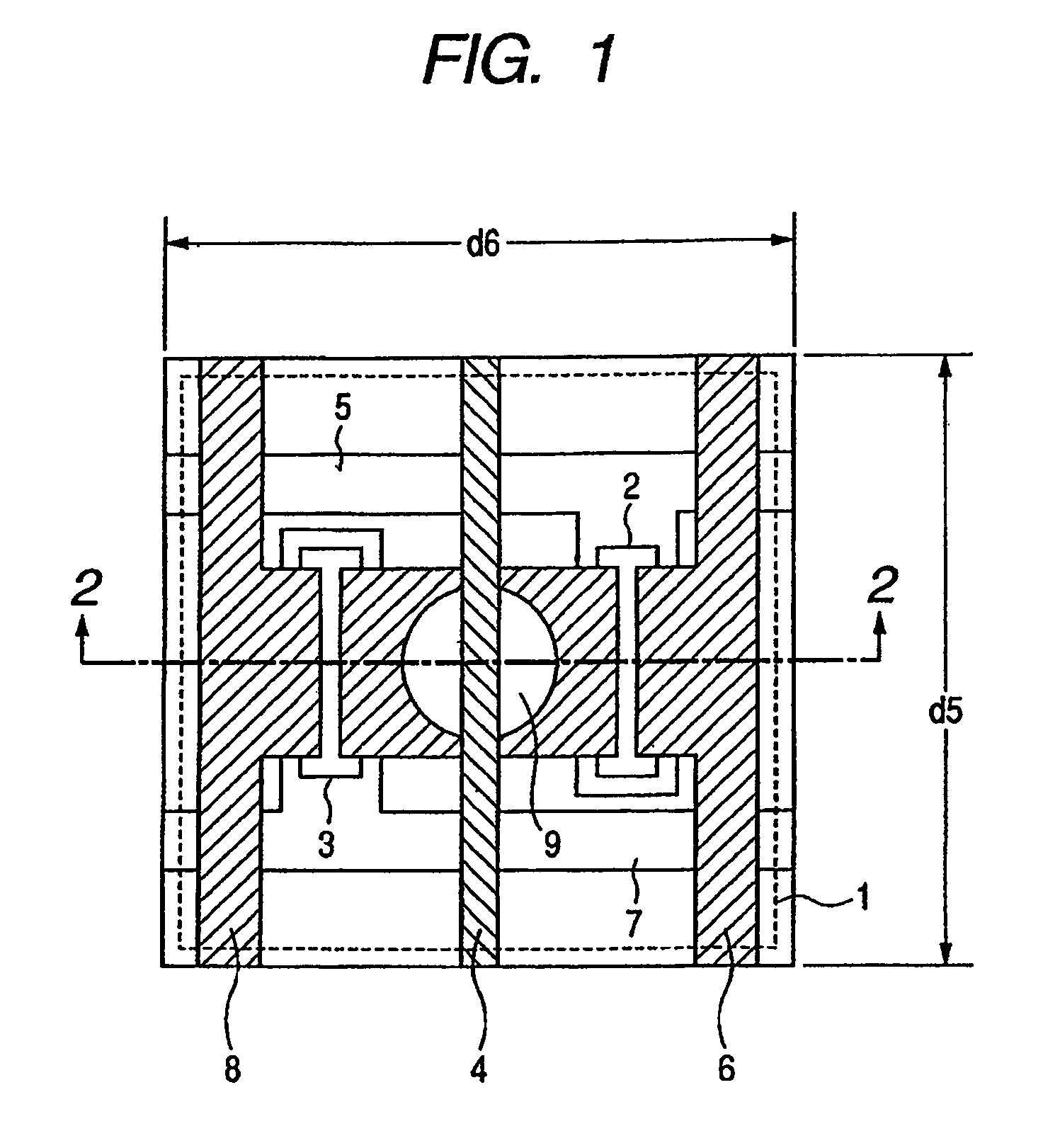
[0034]An radiation imaging apparatus according to a first embodiment of the present invention will be described with reference to the drawings. FIG. 1 is a top plan view of one pixel of the radiation imaging apparatus of the present invention, and FIG. 2 is a sectional view cut along the line 2-2 in FIG. 1.

[0035]The radiation imaging apparatus in the present embodiment includes a lamination-type radiation imaging sensor panel forming a MIS-type photoelectric conversion element that includes a conversion element on the upper part of a transfer switch (transfer TFT) and a reset switch (reset TFT). Further, this apparatus is an indirect-type radiation imaging apparatus including a scintillator for converting the X-rays into light, e.g., visible light, located over these switches.

[0036]A configuration of the radiation detector of the present embodiment will be described with reference to FIGS. 1 and 2.

[0037]In FIG. 1, reference numeral 1 denotes a conversion element such as a photoelect...

second embodiment

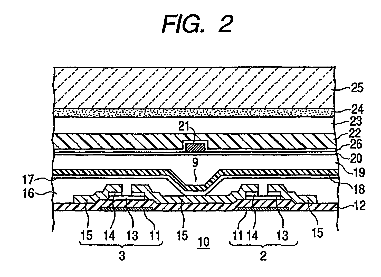
[0045]Hereinafter, a radiation imaging apparatus according to a second embodiment of the present invention will be described with reference to the drawings. FIG. 3 is a top plan view of one pixel of the radiation imaging apparatus of the present embodiment, and FIG. 4 is a sectional view cut along the line 4-4 in FIG. 3.

[0046]The radiation imaging apparatus in the present embodiment has a lamination type radiation imaging apparatus substrate disposed with a MIS-type photoelectric conversion element including a conversion element on the upper part of a transfer switch (transfer TFT) and a reset switch (reset TFT). Further, located over the lamination-type radiation imaging apparatus substrate, it is an indirect radiation imaging apparatus having a scintillator for converting X-rays into light, e.g., visible light. An equivalent circuit diagram of the radiation imaging apparatus of the present embodiment is the same as for the conventional structure described above, and its operation ...

third embodiment

[0059]Hereinafter, a radiation imaging apparatus according to a third embodiment will be described with reference to the drawings. FIG. 5 is a sectional view of the radiation imaging apparatus of the present embodiment, and is a sectional view equivalent to the line 2-2 in FIG. 1. The same component parts as those of FIG. 2 are identified using the same reference number, and description thereof will be omitted.

[0060]The present embodiment relates to a direct-type radiation imaging apparatus using a conversion element that sandwiches a semiconductor layer such as amorphous selenium directly converting corpuscular rays such as X-rays, γ-rays or α-rays and β-rays into light, e.g., visible light, between electrodes in place of the photoelectric conversion element of FIG. 2 showing the first embodiment. The present embodiment describes the case where X-rays are allowed to enter a radiation detector similarly to the first and second embodiments.

[0061]The points of difference between the r...


PUM


Abstract

Pixels including a photoelectric conversion element 1, a signal transfer TFT (thin film transistor) 2 electrically connected to the photoelectric conversion element, and a reset TFT 3 electrically connected to the photoelectric conversion element and for applying a bias to the photoelectric conversion element are two-dimensionally disposed on the insulating substrate, and the photoelectric conversion element 1, signal transfer TFT 2, and reset TFT 3 are electrically connected through a common contact hole 9. A source or drain electrode of the signal transfer TFT 2 and the source or drain electrode of the reset TFT 3 are formed from a common electroconductive layer.

Description

[0001]This Application is a National Stage filing under 35 U.S.C. §371 of International Application No. PCT / JP2007 / 050629, filed Jan. 11, 2007.TECHNICAL FIELD[0002]The present invention relates to an optical imaging apparatus and a radiation imaging apparatus applied to an analyzing instrument and the like that are suitable for use as a medical diagnostic imaging apparatus, a non-destructive inspection apparatus, and the like. Incidentally, in the present specification, the term “radiation” is intended to include not only electromagnetic radiation such as X-rays and γ-rays but also to beams of corpuscular bodies such as α-rays and β-rays. Further, the term “conversion element” refers to a semiconductor element that converts at least a light signal or radiation into an electrical signal.BACKGROUND ART[0003]In recent years, manufacturing technology of liquid crystal display panels using thin film transistors (TFT) has been advancing, and upsizing of the panel and the display unit scre...

Claims


Application Information

Patent Timeline
Patent Type & Authority Patents(United States)
IPC IPC(8): G01T1/24G01T1/20H01L27/146
CPCG01T1/2018H01L27/14603H01L27/14632H01L27/14663G01T1/2006
Inventor ISHII, TAKAMASAMOCHIZUKI, CHIORIWATANABE, MINORU
Owner CANON KK
Why Eureka
Try Eureka