Tracking error signal detection device and optical disc apparatus

a detection device and optical disc technology, applied in the direction of digital signal error detection/correction, instruments, recording signal processing, etc., can solve the problems of difficult to perform this operation accurately, high element sensitivity, and inconvenient high-frequency boost circuits

Inactive Publication Date: 2011-11-29
SONY CORP
View PDF1 Cites 4 Cited by
  • Summary
  • Abstract
  • Description
  • Claims
  • Application Information

AI Technical Summary

Benefits of technology

[0033]Therefore, unlike the technique according to the first example, the technique according to the second example avoids the problem affecting an operation speed caused by data delay time and timing control.
[0051]Furthermore, judging from the nature of the tracking error detection circuit, the full seeking operation performed from the innermost circumference to the outermost circumference of the disc should properly function. Accordingly, the A / D converter should operate with a sampling frequency higher than an RF channel frequency so that aliasing is prevented from being generated even when the full seeking operation is performed.
[0054]It is desirable to provide a tracking error signal detection device capable of realizing a device employing a DPD method as a digital circuit which operates at high speed with high accuracy and an optical disc apparatus.

Problems solved by technology

The high-frequency boost circuit (equalizer) used in the first example described above is configured using a high-order transfer function, and therefore, there arises problems in that a circuit size thereof is large, element sensitivity is high, and the high-frequency boost circuit is not suitable for an analog circuit employing a fine CMOS process having large variation.
However, it is difficult to perform this operation accurately.
Furthermore, although the phase comparator includes a digital gate, the phase comparator is incapable of performing timing control (static timing analysis: STA) utilizing a clock synchronization design which is used in general digital circuits, and therefore, it is difficult to ensure a high-speed stable operation.
Moreover, with this configuration, there arise fundamental problems in that process shrink of analog circuit blocks has not yet caught up with process shrink of digital circuit blocks caused by advancing development of microfabrication processes of semiconductors.

Method used


Image

  • Tracking error signal detection device and optical disc apparatus
  • Tracking error signal detection device and optical disc apparatus
  • Tracking error signal detection device and optical disc apparatus

Examples


first embodiment

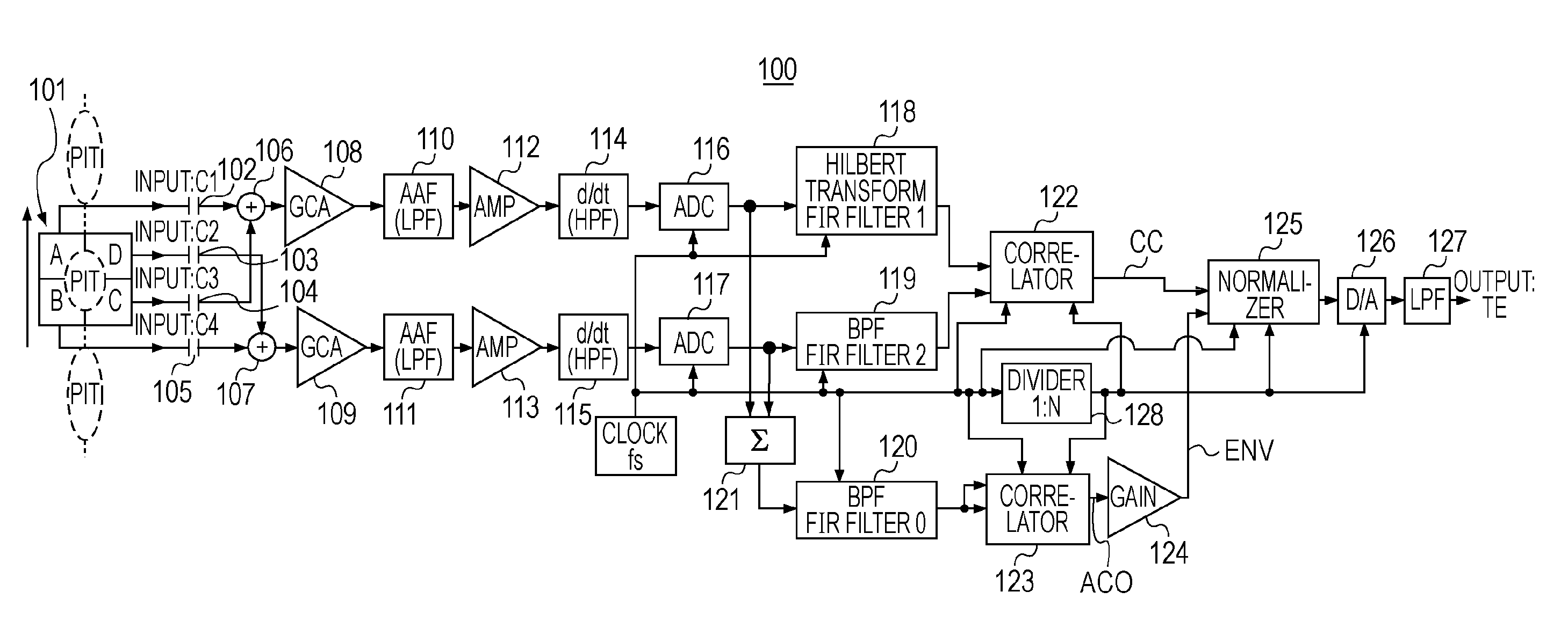
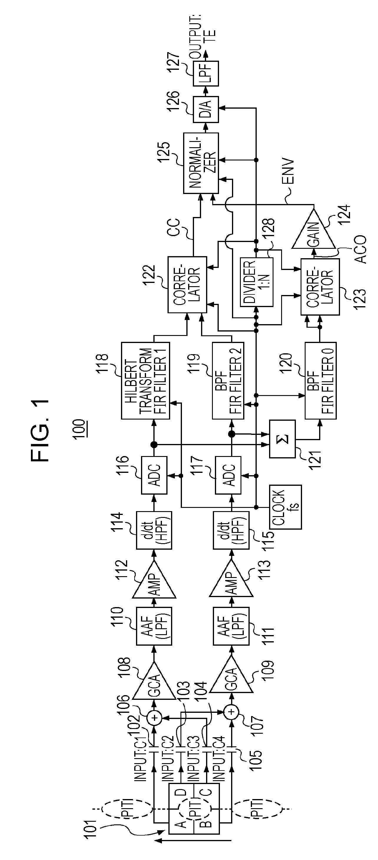
[0078]FIG. 1 is a circuit diagram illustrating a configuration of a tracking error (TE) detection device employing a DPD method according to a first embodiment of the present invention.

[0079]A TE detection device 100 of the first embodiment includes a light-receiving element 101 included in an optical pickup (OPU) of an optical disc, a first AC coupling unit 102, a second AC coupling unit 103, a third AC coupling unit 104, a fourth AC coupling unit 105, a first adder 106, a second adder 107, a first gain control amplifier (GCA) 108, a second GCA 109, a first anti-aliasing filter (AAF) 110, a second AAF 111, a first amplifier 112, a second amplifier 113, a first differentiator 114, a second differentiator 115, a first analog / digital converter (ADC) 116, a second ADC 117, a Hilbert transformer 118, a first delay circuit 119, a second delay circuit 120, a summing circuit 121, a cross-correlator 122, an autocorrelator 123, a gain circuit 124, a normalizer 125, a digital / analog converter...

second embodiment

[0176]FIG. 8 is a circuit diagram illustrating a configuration example of a tracking error (TE) detection device employing a DPD method according to a second embodiment of the present invention.

[0177]A TE detection device 100A according to the second embodiment is different from the TE detection device 100 according to the first embodiment in the following points.

[0178]A first ADC 116 is connected at an output terminal thereof to a first Hilbert transformer 118-1 and a first delay circuit 119-1, and a second ADC 117 is connected at an output terminal thereof to a second Hilbert transformer 118-2 and a second delay circuit 119-2.

[0179]Furthermore, the first Hilbert transformer 118-1 and the second delay circuit 119-2 are connected to a first cross-correlator 122-1 which calculates the correlation between a signal output from the first Hilbert transformer 118-1 and a signal output from the second delay circuit 119-2. Moreover, the second Hilbert transformer 118-2 and the first delay c...

third embodiment

[0196]FIG. 14 is a circuit diagram illustrating a configuration example of a tracking error (TE) detection device employing a DPD method according to a third embodiment of the present invention.

[0197]A TE detection device 500 according to the third embodiment includes a light-receiving element 501 arranged in an optical pickup (OPU) in an optical disc, a first AC coupling unit 502 to a fourth AC coupling unit 505, a first GCA 506 to a fourth GCA 509, a first AAF 510 to a fourth AAF 513, a first amplifier 514 to a fourth amplifier 517, a first differentiator 518 to a fourth differentiator 521, a clock generator 522, a first ADC 523 to a fourth ADC 526, a first Hilbert transformer 527, a second Hilbert transformer 528, a first delay circuit 529 to a third delay circuit 531, a summing circuit 532, a first cross-correlator 533, a second cross-correlator 534, an adder 535, an autocorrelator 536, a gain circuit 537, a normalizer 538, a DAC 539, an LPF 540, and a divider 541.

[0198]The ligh...


PUM

PropertyMeasurementUnit
differential phase detection methodaaaaaaaaaa
phaseaaaaaaaaaa
phase shiftaaaaaaaaaa

Abstract

A tracking error signal detection device employing a differential phase detection method includes first and second differentiators which remove direct current components in first and second signal groups in which a phase difference between the first and second signal groups changes in accordance with a tracking error signal, and which differentiate the first and second signal groups, first and second analog / digital converters which sample and quantize signals output from the first and second differentiators, respectively, a Hilbert transformer performing a 90-degree phase shift on one of signals output from the first and second analog / digital converters, a delay circuit delaying one of the signals output from the second and first analog / digital converters by an amount of delay equal to that caused by the Hilbert transformer, and a phase comparator calculating a phase difference between a signal output from the Hilbert transformer and a signal output from the delay circuit.

Description

CROSS REFERENCES TO RELATED APPLICATIONS[0001]The present invention contains subject matter related to Japanese Patent Application JP 2007-171689 filed in the Japanese Patent Office on Jun. 29, 2007, the entire contents of which are incorporated herein by reference.BACKGROUND OF THE INVENTION[0002]1. Field of the Invention[0003]The present invention relates to a tracking error (TE) detection device using a DPD (differential phase detection) method which is employed in an optical disc apparatus, for example, and the optical disc apparatus.[0004]2. Description of the Related Art[0005]In general, optical controllers include TE (tracking error) detection devices (circuits) employing DPD methods in order to generate tracking error signals in ROM discs. The TE detection devices employing the DPD methods are currently realized by analog circuits which operate at high speed and which have high accuracies (refer to Japanese Patent No. 3336778, Japanese Unexamined Patent Application Publicati...

Claims


Application Information

Patent Timeline
Patent Type & Authority Patents(United States)
IPC IPC(8): G11B7/00
CPCG11B7/0906G11B7/0941G11B7/0943
Inventor KOBAYASHI, NOBUYOSHI
Owner SONY CORP
Why Eureka
Try Eureka