Micro-granular delay testing of configurable ICs

a micro-granular delay and configurable technology, applied in the direction of instruments, computations using denominational number representations, pulse techniques, etc., can solve the problems of individual transistors operating more slowly than required, affecting the operation of the ic, and being subject to large transistor to transistor variation, so as to accurately measure the performance of the shorter test path and reduce the minimum testable duration

Active Publication Date: 2011-12-06
ALTERA CORP
View PDF142 Cites 34 Cited by
  • Summary
  • Abstract
  • Description
  • Claims
  • Application Information

AI Technical Summary

Benefits of technology

[0036]In such an environment, the configurable storage elements provide plentiful configurable “capture” elements that are able to store data at various points along a test path, thus breaking a long signal path into multiple smaller paths and allowing micro-granular testing of signal-path delay. The data stored by the capture elements may be read out using the configuration / debug network in order to verify the operation of the IC.
[0038]The test method (1) loads configuration data to the configurable circuits to specify the desired operation of the configurable circuits during test, (2) configures the configuration / debug network to allow access to the desired test points (e.g., capture elements) within the IC, (3) operates the IC in “user” mode to exercise the circuitry (i.e., operated as in a final application after configuring the IC to perform functionality specified by a user design), and (4) reads the data in the storage elements to verify the operation of the circuitry under test. In this manner, the method allows a large number of shorter paths to be tested in parallel while operating under realistic final application conditions.
[0043]In some embodiments, the capture elements are observable as memory-mapped resources accessed via a bus. Such a bus may be included in (or accessed using) the configuration / debug network in some embodiments. The accessibility of these observation nodes is limited by the address decode of the bus logic, not by the connection of observation nodes to external device IOs (e.g., I / O pads, I / O pins, etc.). This allows a very large number of observation nodes to be tested on a particular IC without requiring a large number of test pads or pins. In addition, the bus logic allows multiple capture nodes to be verified simultaneously.
[0045]To more accurately measure the performance of the shorter test paths, some embodiments operate the IC using a sub-cycle operating scheme, whereby multiple operational sub-cycles (e.g., four, eight, etc.) occur during each user design cycle. By testing the IC using sub-cycle operation, signal paths that have delays that are fractions of a user design cycle may be used. In addition to testing the circuitry using a sub-cycle operating scheme, some embodiments vary the clock frequency or utilize multiple phase-shifted clock signals in order to further reduce the minimum testable duration.
[0050]Some embodiments allow more precise measurement of power supply variation within an IC. The use of launch-capture testing allows many delay measurements (e.g., >100,000) to be taken simultaneously within a single IC. Because very fine resolution delay measurements may be made at a very large number of locations on the IC, some embodiments may identify a group of circuits under test that have increased delay. Thus, the locations of high resistance metal supply connections may be identified. By analyzing the amount of change in the delay with respect to the typical value the resistance of the metal can be determined.
[0052]Measurement of clock skew within an IC is another parameter that may be more accurately measured using launch-capture testing. Various circuits of the IC may be programmed to be driven by different clock sources. The different clock sources will have varying amounts of clock skew. Comparing delay measurements taken using different clock sources allows the skew of the clock sources to be determined.

Problems solved by technology

During the manufacture of a configurable IC it is possible for flaws to affect the operation of the IC.
In addition to flaws, configurable ICs that use minimum width (or near-minimum width) transistors for a particular manufacturing technology are subject to large transistor to transistor variation.
These variations can cause individual transistors to operate more slowly than required.
In some cases the flaws and / or variations are manifested as malfunctioning circuit elements (e.g., stuck outputs).
In other cases, the flaws and / or variations are manifested as substandard performance (e.g., excessive propagation delay).
Any slow or non-functioning circuit element may potentially render the configurable IC unusable.
The effect of these stresses on the performance of the IC is not fully measured using traditional IC test methods.

Method used


Image

  • Micro-granular delay testing of configurable ICs
  • Micro-granular delay testing of configurable ICs
  • Micro-granular delay testing of configurable ICs

Examples


Embodiment Construction

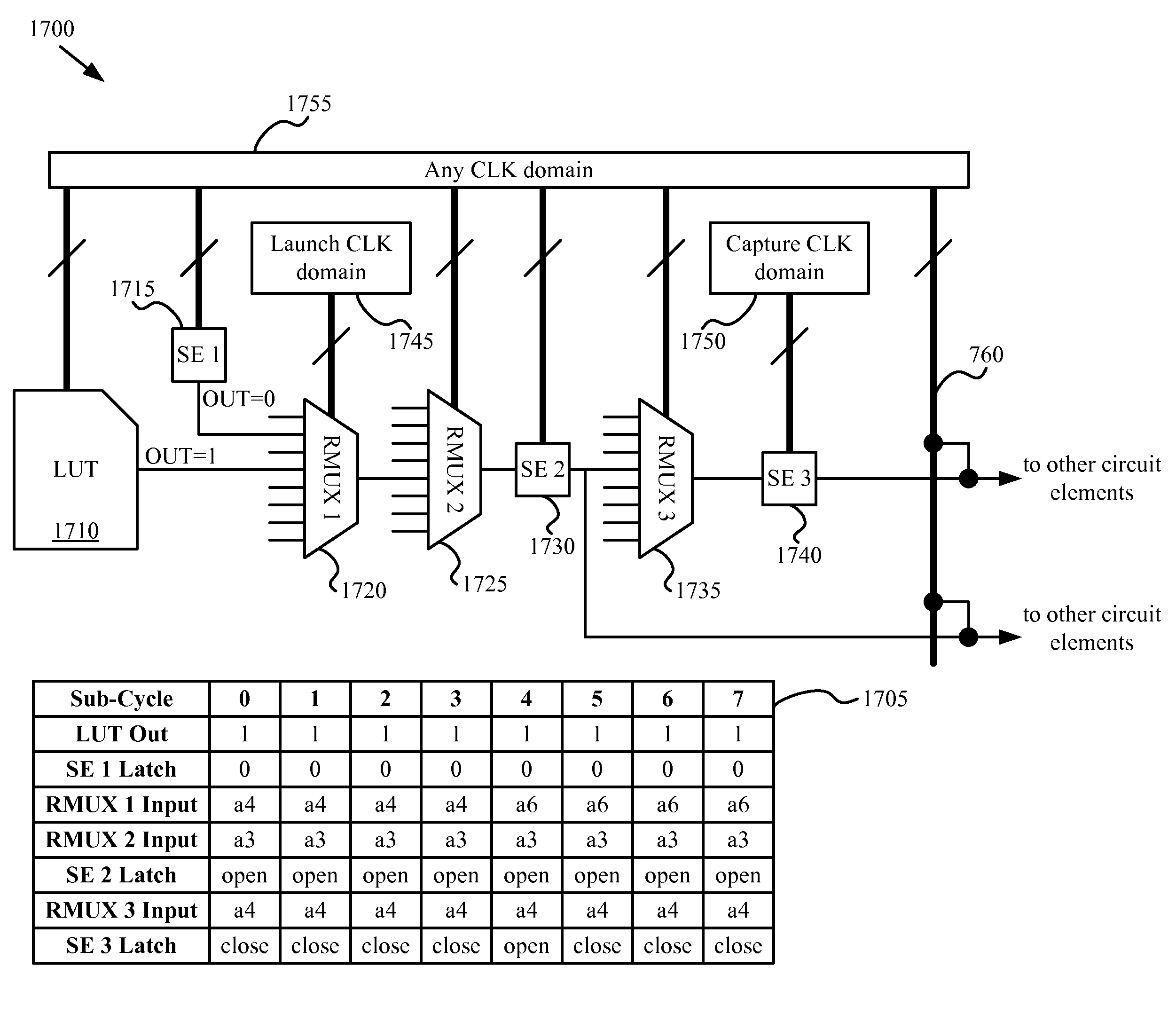
[0054]In the following description, numerous details are set forth for purpose of explanation. However, one of ordinary skill in the art will realize that the invention may be practiced without the use of these specific details. For instance, well-known structures and devices are shown in block diagram form in order not to obscure the description of the invention with unnecessary detail.

[0055]A method of testing a configurable integrated circuit (“IC”) is provided by some embodiments. Such configurable ICs may have a primary circuit structure including configurable logic circuits for configurably performing logic functions, a configurable routing fabric for configurably connecting the circuits of the IC, and / or configurable storage elements placed throughout the configurable routing fabric for configurably storing signals passed along the routing fabric. In addition these configurable ICs may have a secondary circuit structure including a configuration / debug network (alternatively r...


PUM


Abstract

A method for testing a set of circuitry in an integrated circuit (IC) is described. The IC includes multiple configurable circuits for configurably performing multiple operations. The method configures the IC to operate in a user mode with a set of test paths that satisfies a set of evaluation criteria. Each test path includes a controllable storage element for controllably storing a signal that the storage element receives. The method operates the IC in user mode. The method reads the values stored in the storage elements to determine whether the set of circuitry is operating within specified performance limits.

Description

CLAIM OF BENEFIT TO PRIOR APPLICATION[0001]The present Application claims the benefit of U.S. Provisional Application 61 / 244,425, entitled “Launch-Capture Testing of Configurable ICs,” filed on Sep. 21, 2009. U.S. The present Application also claims the benefit of U.S. Provisional Application 61 / 320,692, entitled “Micro-Granular Delay Testing of Configurable ICs,” filed on Apr. 2, 2010. Provisional Patent Applications 61 / 244,425 and 61 / 320,692 are incorporated herein by reference.BACKGROUND[0002]Configurable integrated circuits (“ICs”) can be used to implement circuit functionality designed by a user (“user design”) on an IC without having to fabricate a new IC for each design. One example of a configurable IC is a field programmable gate array (“FPGA”). A configurable IC has several circuits for performing different operations. Configurable circuits can be configured by configuration data to perform a variety of different operations. These circuits can range from logic circuits (e....

Claims


Application Information

Patent Timeline
Patent Type & Authority Patents(United States)
IPC IPC(8): H03K19/00
CPCG01R31/3016G01R31/31725H03K19/17764G01R31/3177G01R31/318516G01R31/318519
Inventor FOX, BRIAN
Owner ALTERA CORP
Why Eureka
Try Eureka