Ultra-wideband assembly system and method

a technology of ultra-wideband and assembly system, applied in waveguides, instruments, therapy, etc., can solve the problems of reducing the transmission signal power, the inductance of the tapered coil cannot be made insufficiently, and the type of singe layer cannot be sufficiently high, so as to achieve the effect of minimizing the perturbation of the electric field

a technology of ultra-wideband and assembly system, applied in waveguides, instruments, therapy, etc., can solve the problems of reducing the transmission signal power, the inductance of the tapered coil cannot be made insufficiently, and the type of singe layer cannot be sufficiently high, so as to achieve the effect of minimizing the perturbation of the electric field

US8072773B2Active Publication Date: 2011-12-06AMERICAN TECH CERAMICS CORP

Image

  • Ultra-wideband assembly system and method
  • Ultra-wideband assembly system and method
  • Ultra-wideband assembly system and method

Examples


Embodiment Construction

[0027]The present invention generally relates to electrical circuits and more specifically, the present invention relates to ultra-wideband assembly systems and methods that improve operational frequencies of electrical circuits.

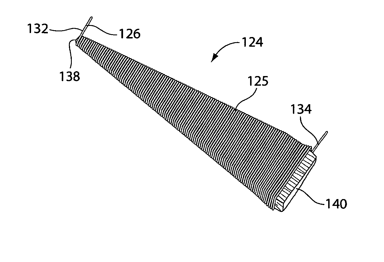
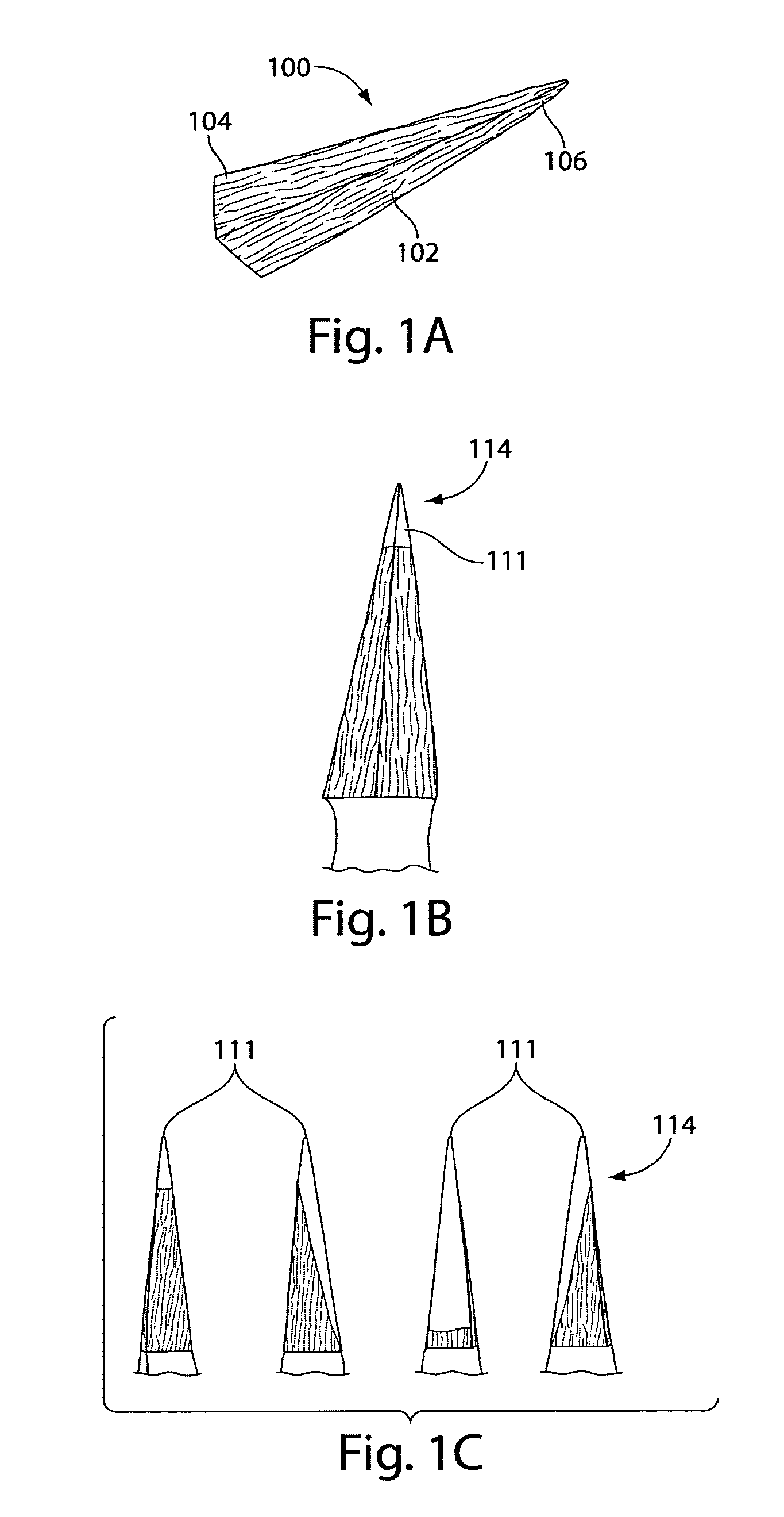
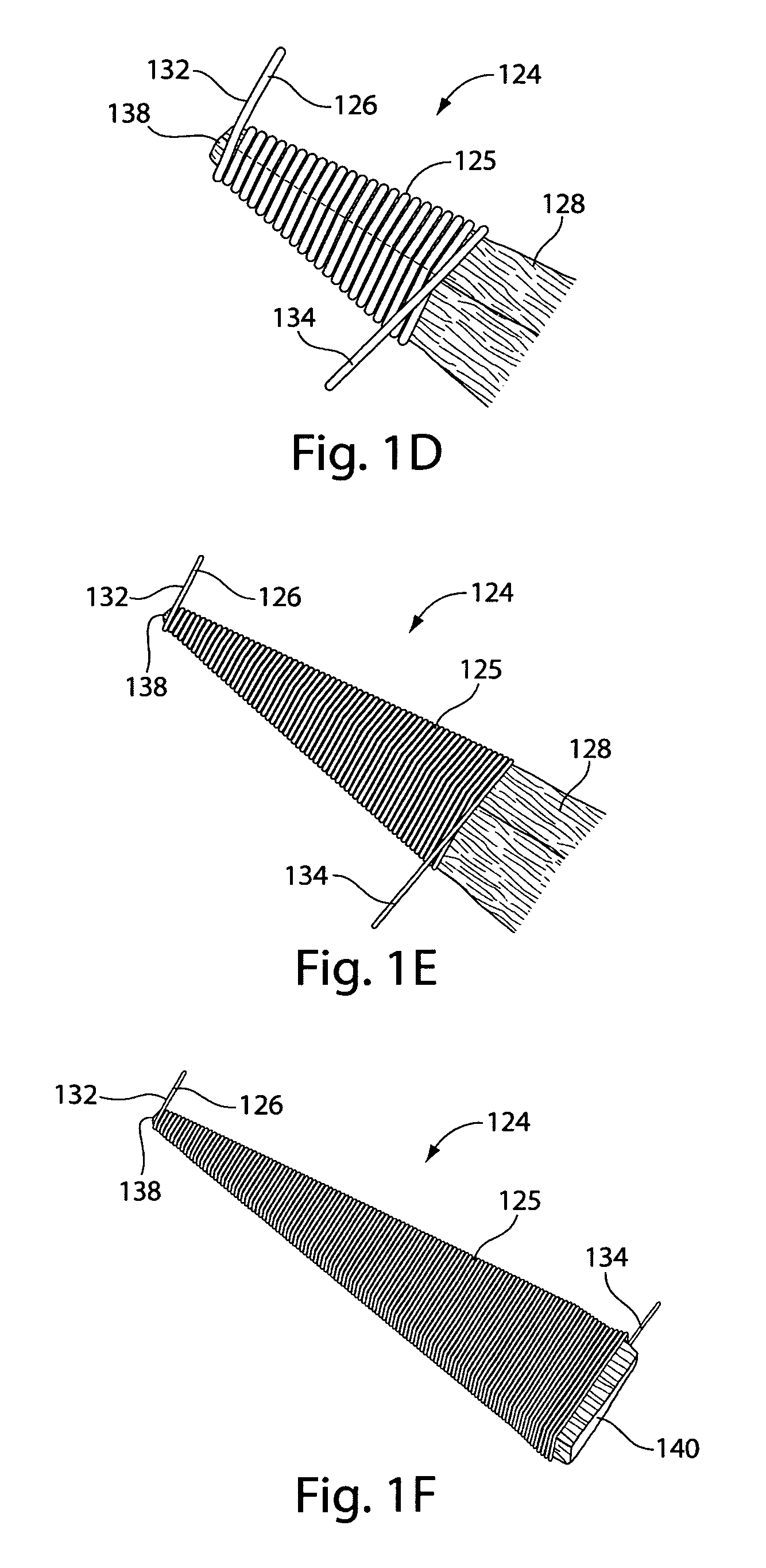
[0028]In some embodiments, the present invention relates to a non-conductive tapered core assembly for mounting the core in an electrical circuit to improve operational frequency range. FIGS. 1a-h illustrate an exemplary non-conductive tapered core 100, according to some embodiments of the present invention. The core 100 has a shape of a pyramidelepiped (i.e., a pyramid having a parallelogram base). In some embodiments, the core 100 can be a square, a rectangular, a triangular, a polygonal, or any other type pyramidal or other multi-dimensional structure. In some embodiments, the core 100 can be manufactured from powdered iron particles.

[0029]FIG. 1a illustrates an exemplary powdered core 100, according to some embodiments of the present invention. As illust...


PUM


Abstract

An ultra-wideband assembly is provided. The assembly includes a non-conductive tapered core having a conductive wire wound on an outer surface of the non-conductive tapered core, a low-frequency inductor coupled to the non-conductive tapered core via the distal end of the conductive wire and configured to allow mounting of the non-conductive tapered core at an angle with respect to the circuit board. The low frequency inductor is being disposed on a dielectric board configured to be coupled to the circuit board. The assembly includes an ultra-wideband capacitor coupled to the non-conductive tapered core via the proximate end of the conductive wire, the ultra-wideband capacitor being also coupled to the transmission line on the dielectric board.

Description

BACKGROUND OF THE INVENTION[0001]1. Field of the Invention[0002]The present invention generally relates to electrical circuits. Specifically, the present invention relates to ultra-wideband assembly systems and methods that provide a wide range of operational frequencies with low insertion loss.[0003]2. Background of the Invention[0004]With the development of multi-media technology, there is an increasing demand for constructing optical communication networks that are capable of providing transmissions at high speeds and accommodating large volumes of information. There is also a demand to provide such transmissions at lowered costs and over long distances. Various conventional systems that provide transmission high rates between 10 Gb / s to over 40 Gb / s have been developed or are currently under development.[0005]To accommodate such high speeds of transmission, electronic circuits having bias-tee (also referred to as “bias-T”) packages disposed on transmitter-receivers have been dev...

Claims


Application Information

Patent Timeline
06 Dec 2011
Publication
US8072773B2
IPC
H05K7/00
CPC
H01F17/04; H01F27/06; H03H7/1741; H01G4/40; H03H7/0115; H03H7/0138; H01F2005/006; H05K1/0243
Inventors
MRUZ, JOHN