Method and apparatus for layout independent test point placement on a printed circuit board

Active Publication Date: 2006-04-27
KEYSIGHT TECH
View PDF31 Cites 3 Cited by
  • Summary
  • Abstract
  • Description
  • Claims
  • Application Information

AI Technical Summary

Benefits of technology

[0013] The present invention solves the conflict problems faced by traditional techniques for test access point placement on printed circuit boards by minimizing the perturbations of traces in the x- and y-dimensions and taking advantage of the z-dimension. In particular, the invention utilizes trace thickness to implement test access points, thereby allowing test access point placement almost anywhere along the trace. This in turn allow

Problems solved by technology

Such printed circuit assembly testing is generally performed with automated in-circuit testers or ICT's and requires complex tester resources.
Lower diameter targets are increasingly difficult to hit reliably and repeatably, especially when a test fixture may contain several thousand such probes.
It is always desirable to use larger diameter targets, but this is in fundamental conflict with the industry trend towards higher densities and smaller geometry devices.
When traditional test probe targets are added, this causes discontinuities in the controlled impedances and may damage signal fidelity.
However, routing signals on a crowded printed circuit board necessitates curves and bends in the path, which makes matching lengths and symmetries more difficult.
Signals may also have to traverse connectors, which add to the difficulties.
Such changes to high-density boards in many cases, may not be practical, as there may not be any room to move traces.
If any of the signal traces also ha

Method used


Image

  • Method and apparatus for layout independent test point placement on a printed circuit board
  • Method and apparatus for layout independent test point placement on a printed circuit board
  • Method and apparatus for layout independent test point placement on a printed circuit board

Examples


Example

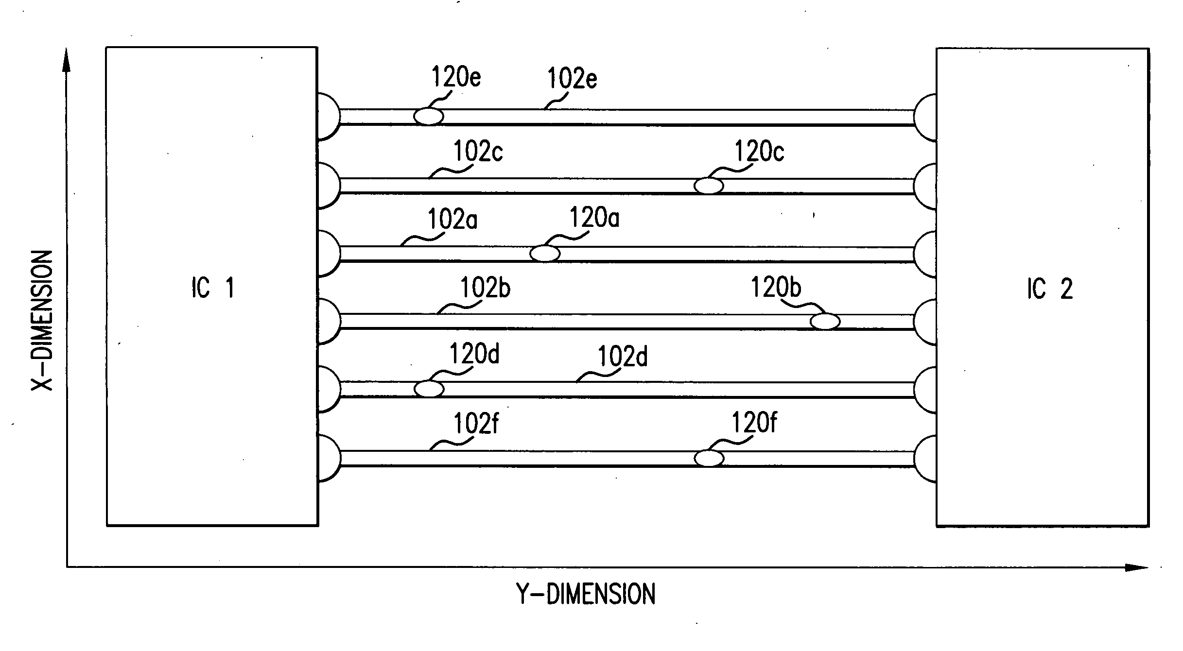
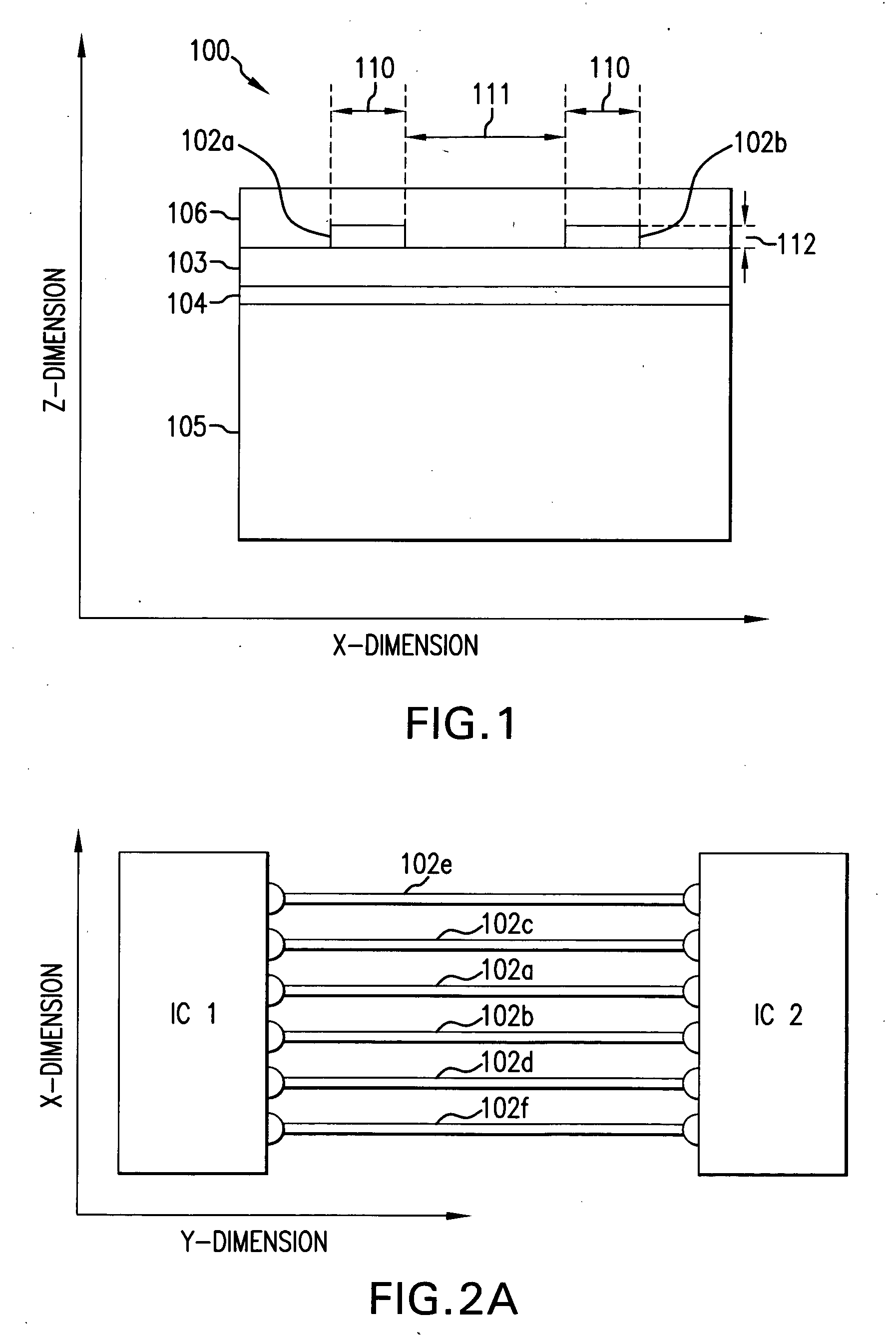
[0036] Turning now in detail to the invention, on a trace defined in an x-, y-, z-coordinate system where the x-dimension represents the trace width, the y-dimension represents the trace length, and the z-dimension represents the trace thickness, it will be recognized by those skilled in the art that present techniques for test access point placement on a printed circuit board utilize only the x- and y-dimensions. The present invention takes a different approach by taking advantage of the z-dimension, that is, the trace thickness. In this regard, the test access point structure of the invention is a localized “high point” on a printed circuit board trace that does not significantly perturb the impedance of the trace and that can be targeted with a probe. Throughout this specification, test access point structure and bead probe structure are used interchangeably.

[0037]FIG. 3 illustrates an exemplary embodiment of a test access point structure implemented in accordance with the inven...


PUM


Abstract

A layout independent test access point structure for accessing test points of a printed circuit board and method of fabrication thereof is presented. Each test access point structure is conductively connected to various locations along a trace at a test access point and above an exposed surface of the printed circuit board to be accessible for probing by a fixture probe.

Description

REFERENCE TO RELATED PATENT DOCUMENTS [0001] The subject matter of this patent application is related to that of U.S. patent application Ser. No. 10 / 670,649 entitled Printed Circuit Board Test Access Point Structures And Methods For Making The Same filed Sep. 24, 2003 by Kenneth P. Parker, Ronald J. Peiffer and Glen E. Leinbach and assigned to Agilent Technologies, Inc., which teaches the basic concepts of bead probes or test access point structures on a printed circuit board and is hereby incorporated herein by reference.BACKGROUND OF THE INVENTION [0002] Printed circuit assemblies (PCA's) are typically tested after manufacture to verify the continuity of traces between pads and vias on the board and to verify that components loaded on the PCA perform within specifications. Such printed circuit assembly testing is generally performed with automated in-circuit testers or ICT's and requires complex tester resources. The tester hardware must generally be capable of probing conductive ...

Claims


Application Information

Patent Timeline
IPC IPC(8): G01R31/26
CPCG01R31/281G01R31/2818
Inventor PARKER, KENNETH P.
Owner KEYSIGHT TECH
Why Eureka
Try Eureka