Method and apparatus for manufacturing and probing printed circuit board test access point structures

a technology of access point structure and printed circuit board, which is applied in the direction of printed circuit manufacture, circuit inspection/indentification, instruments, etc., can solve the problems of increasing difficulty in reliably and repeatably hitting lower diameter targets, increasing difficulty in matching length and symmetries, and requiring complex tester resources

Active Publication Date: 2009-03-17
KEYSIGHT TECH
View PDF9 Cites 3 Cited by
  • Summary
  • Abstract
  • Description
  • Claims
  • Application Information

AI Technical Summary

Benefits of technology

[0009]The present invention solves the conflict problems faced by traditional techniques for test access point placement on printed circuit boards by minimizing the perturbations of traces in the x- and y-dimensions and taking advantage of the z-dimension. In particular, the invention utilizes trace thickness to implement test access points, thereby allowing test access point placement almost anywhere along the trace. This in turn allows the ability to design printed circuit boards with test access point placement according to the positions of fixture probes of a given test fixture, rather than vice versa as in the prior art.

Problems solved by technology

Such printed circuit assembly testing is generally performed with automated in-circuit testers or ICT's and requires complex tester resources.
Lower diameter targets are increasingly difficult to hit reliably and repeatably, especially when a test fixture may contain several thousand such probes.
It is always desirable to use larger diameter targets, but this is in fundamental conflict with the industry trend towards higher densities and smaller geometry devices.
However, routing signals on a crowded printed circuit board necessitates curves and bends in the path, which makes matching lengths and symmetries more difficult.
Signals may have to traverse connectors, which add to the difficulties.
Additional difficulties arise when testing is considered.
These conflicts lead to either a compromise in controlled impedance integrity, or a forced reduction in target placement with a resulting reduction in testability.
As signal speeds continue to rise and board densities increase, this problem will only get worse.

Method used


Image

  • Method and apparatus for manufacturing and probing printed circuit board test access point structures
  • Method and apparatus for manufacturing and probing printed circuit board test access point structures
  • Method and apparatus for manufacturing and probing printed circuit board test access point structures

Examples


Embodiment Construction

[0042]This invention relates to U.S. patent application Ser. No. 10 / 670,649 entitled Printed Circuit Board Test Access Point Structures And Methods For Making The Same filed Sep. 24, 2003 by Kenneth P. Parker, Ronald J. Peiffer and Glen E. Leinbach and assigned to Agilent Technologies, Inc., which teaches the basic concepts of bead probes or test access point structures on a printed circuit board and is incorporated herein by reference.

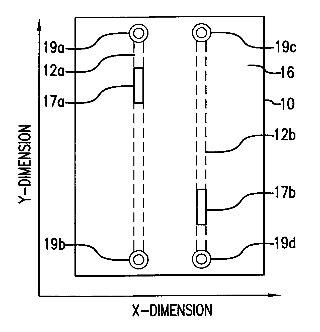
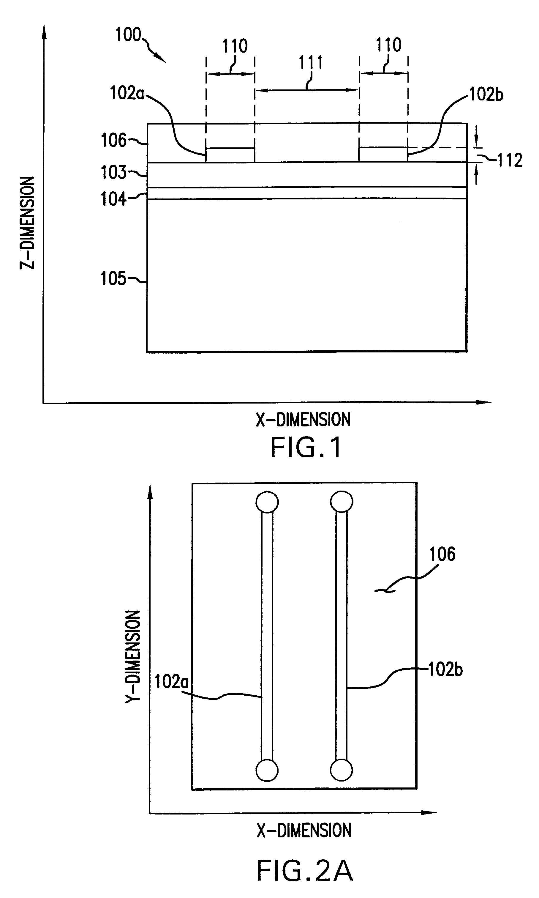
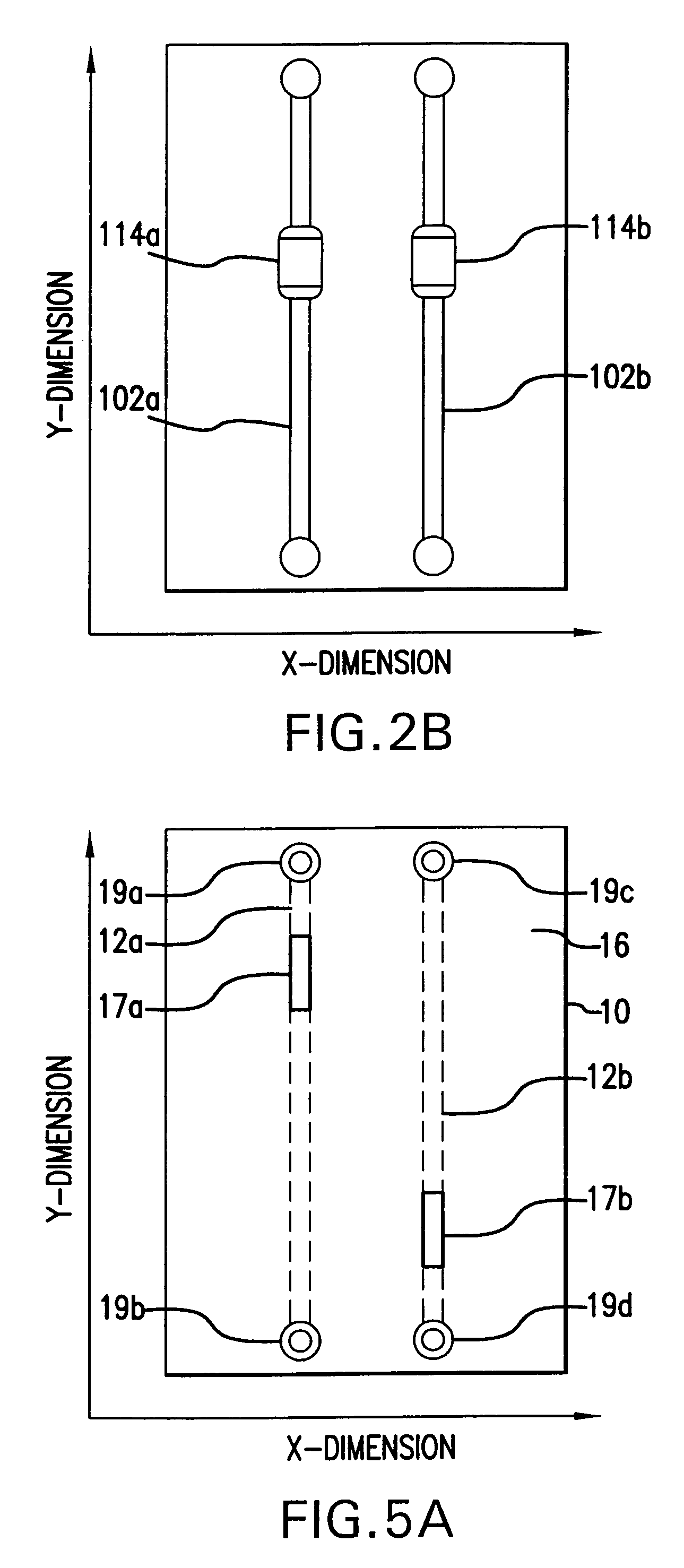
[0043]Turning now in detail to the invention, on a trace defined in an x-, y-, z-coordinate system where the x-dimension represents the trace width, the y-dimension represents the trace length, and the z-dimension represents the trace thickness, it will be recognized by those skilled in the art that present techniques for test access point placement on a printed circuit board utilize only the x- and y-dimensions. The present invention takes a different approach by taking advantage of the z-dimension, that is, the trace thickness. In this regard, the t...


PUM


Abstract

A test access point structure for accessing test points of a printed circuit board and method of fabrication thereof is presented. Each test access point structure is conductively connected to a trace at a test access point and above an exposed surface of the printed circuit board to be accessible for probing by a fixture probe. The test access point structure may be designed and manufactured to permit deformation of the test access point structure upon initial probing of the test access point structure with a fixture probe to ensure electrical contact between the fixture probe and the test access point structure.

Description

BACKGROUND OF THE INVENTION[0001]Printed circuit assemblies (PCA's) are typically tested after manufacture to verify the continuity of traces between pads and vias on the board and to verify that components loaded on the PCA perform within specifications. Such printed circuit assembly testing is generally performed with automated in-circuit testers or ICT's and requires complex tester resources. The tester hardware must generally be capable of probing conductive pads, vias and traces on the board under test.[0002]In-circuit testers (ICT) have traditionally used “bed-of-nails” (BON) access to gain electrical connectivity to circuit wiring (traces, nets, pads) for control and observation capability needed for testing. This necessitates having access points within the layout of circuit nets that can be targets for ICT probes. Test access points are usually circular targets with 28 to 35 mil diameter that are connected to traces on the printed circuit board. In some cases these targets ...

Claims


Application Information

Patent Timeline
Patent Type & Authority Patents(United States)
IPC IPC(8): H05K1/00
CPCG01R31/2818H05K1/0268H05K3/3452H05K3/3457H05K2203/0278H05K2203/043
Inventor PARKER, KENNETH P.JACOBSEN, CHRIS R.
Owner KEYSIGHT TECH
Why Eureka
Try Eureka