Cooling apparatus for semiconductor chips

a cooling apparatus and semiconductor chip technology, applied in the direction of electrical apparatus construction details, light and heating apparatus, basic electric elements, etc., can solve the problems of inconvenient operation, inconvenient operation, and inability to meet the requirements of the application, so as to reduce the cost of manufacturing and increase the chip output.

Active Publication Date: 2011-12-20
FUJI ELECTRIC CO LTD
View PDF17 Cites 131 Cited by
  • Summary
  • Abstract
  • Description
  • Claims
  • Application Information

AI Technical Summary

Benefits of technology

[0014]wherein the radiation fins are configured for causing the cooling efficiency thereof to increase in the flow direction of the coolant from the inflow port toward the outflow port.
[0017]By configuring the radiation fins such that the cooling efficiencies thereof are not equal to each other in the coolant flow direction, in the manner described above, the temperatures, at which the semiconductor chips output their respective maximum outputs, are rendered close to each other. Therefore, the derating due to the temperature unbalance is avoided and a larger chip output is enabled.

Problems solved by technology

Although the other semiconductor chips can make a larger output current flow, the output currents thereof are limited to the output current from the semiconductor chip, the temperature of which is the highest.
Therefore, the other semiconductor chips tend to be undesirably limited in their output.
However, the disposition of many inflow ports and outflow ports complicates the structure.

Method used


Image

  • Cooling apparatus for semiconductor chips
  • Cooling apparatus for semiconductor chips
  • Cooling apparatus for semiconductor chips

Examples


first embodiment

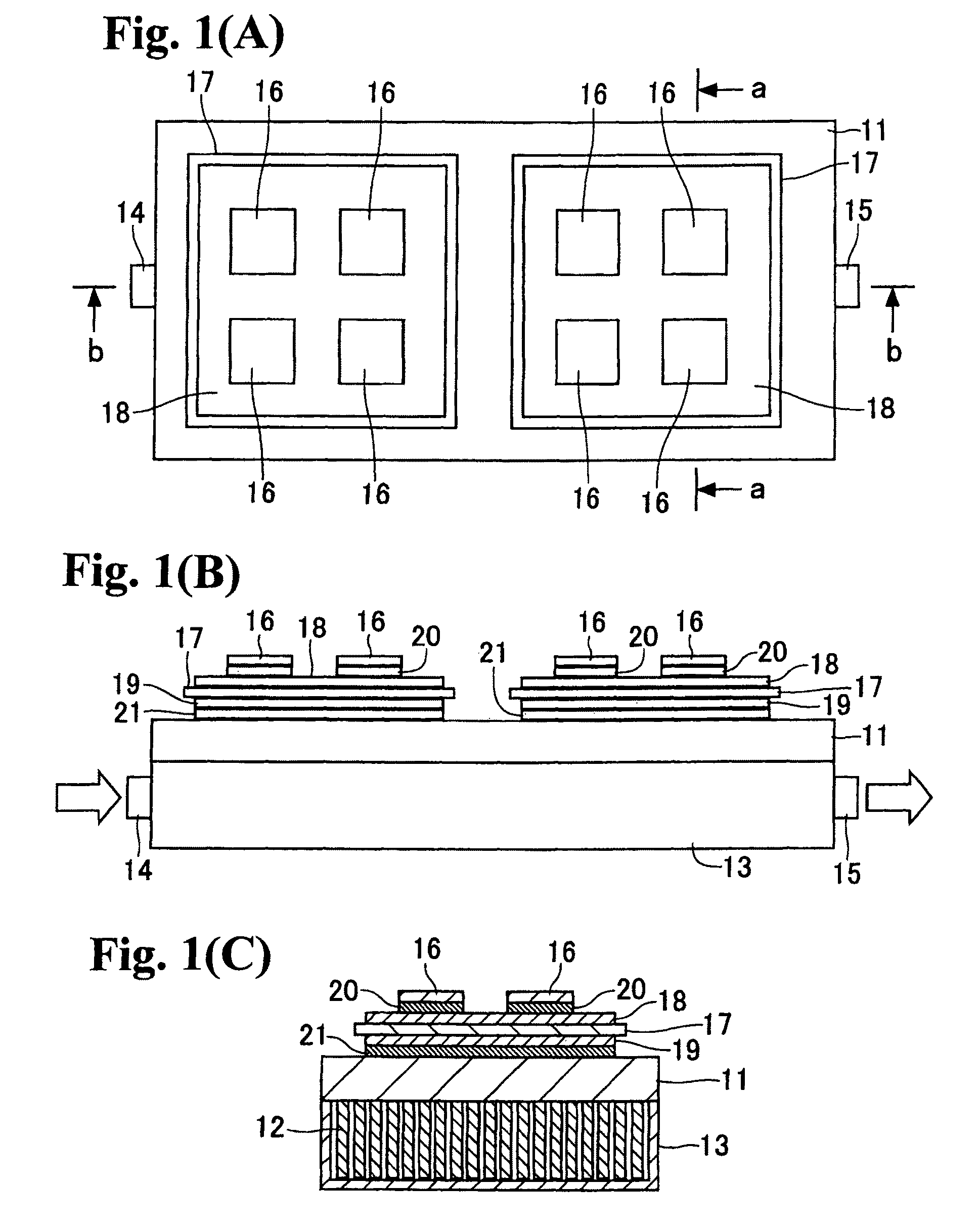
[0041]FIG. 1(A) is a top plan view of a cooling apparatus for semiconductor chips (hereinafter referred to as a “cooling apparatus”) according to the invention. FIG. 1(B) is a side plan view of the cooling apparatus shown in FIG. 1(A); and FIG. 1(C) is a cross sectional view of the cooling apparatus along a-a of FIG. 1(A).

[0042]The electrical connections on the semiconductor chips, the terminals for external connections, the casing, and the sealant are not shown in these drawings.

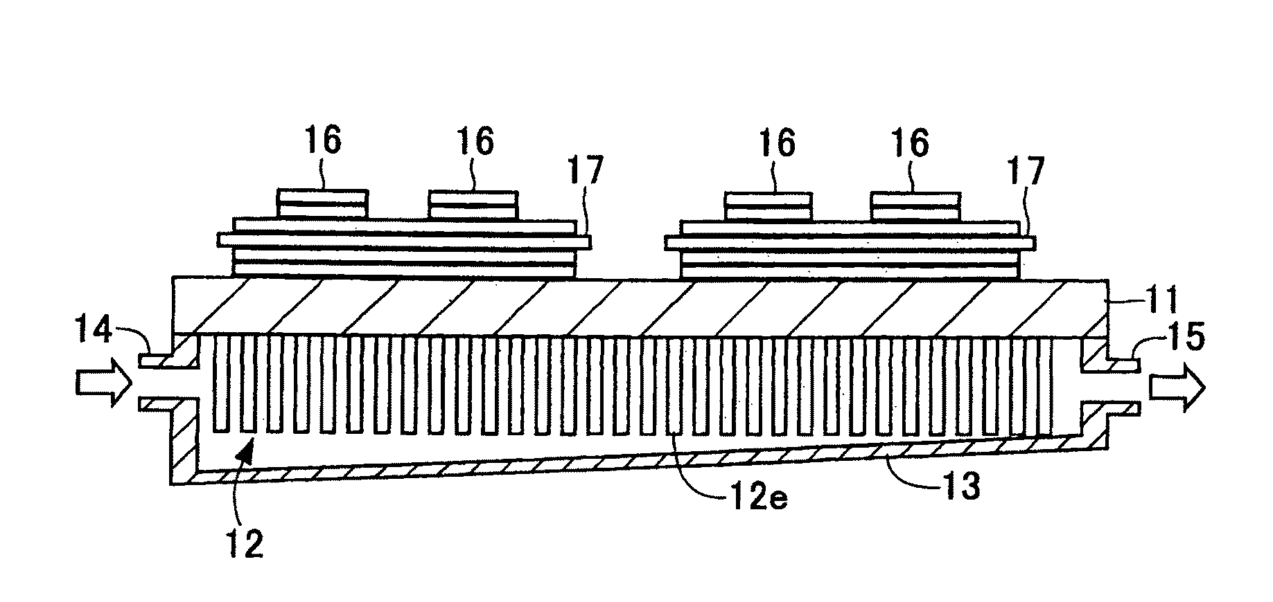
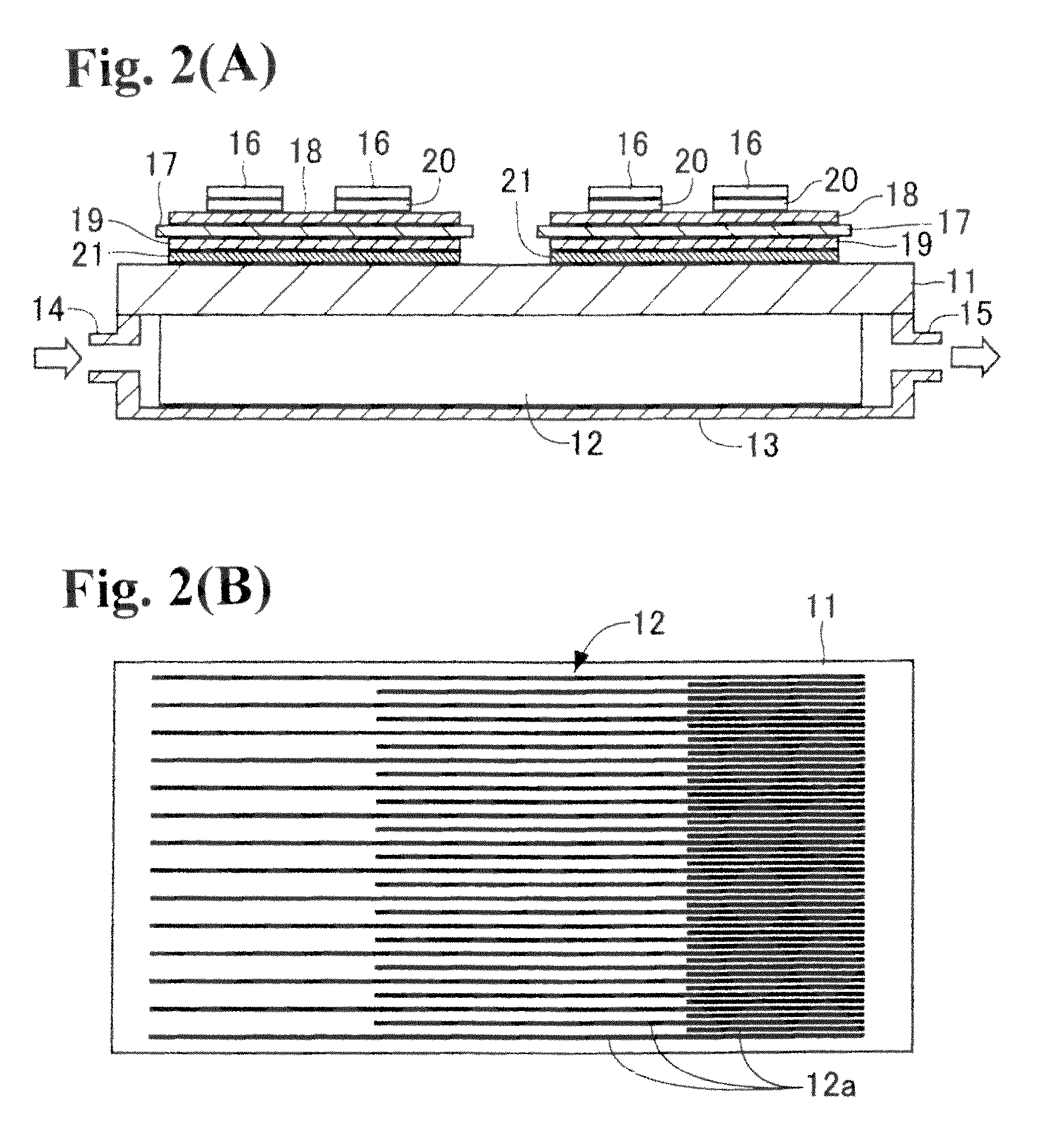
[0043]The cooling apparatus according to the first embodiment of the invention includes metal base 11, on which heat sources are mounted, radiation fins 12 are formed on the under surface of metal base 11 and integrated with metal base 11 into a unit, and a duct cover 13 is bonded to metal base 11 such that duct cover 13 surrounds radiation fins 12 and forms a duct (flow path) for a coolant. The radiation fins 12 are made of a metal or an alloy such as copper, a copper alloy, aluminum, and an aluminum alloy...

second embodiment

[0061]In the cooling apparatus according to the invention, radiation fins 12 are pin-shaped (viz., cylindrical) fins 12e arranged along the coolant flow direction in the duct and bonded / connected to metal base 11. In FIG. 5(A), pin-shaped fins 12e having the same diameter and the same height are arranged such that the pitch between the adjacent pin-shaped fins 12e is made shorter from inflow port 14 toward outflow port 15. Due to the fin arrangement described above, the total surface area of pin-shaped fins 12e on a unit area of metal base 11 (hereinafter referred to as the “surface area density of pin-shaped fins 12e”) is gradually higher from inflow port 14 toward outflow port 15.

[0062]The radiation fins in the cooling apparatus shown in FIG. 5(B) comprise a first modified example of radiation fin 12 shown in FIG. 5(A). In FIG. 5(B), radiation fins 12 are pin-shaped fins 12e having the same height and arranged at the same pitch in a section of the duct. The diameter of pin-shaped ...

third embodiment

[0064]FIG. 6 is a top plan view showing the radiation fins in a cooling apparatus according to the invention.

[0065]In the cooling apparatus according to this third embodiment, radiation fins 12 include sheet-shaped fins 12a shown in FIG. 2(B), and pin-shaped fins 12e shown in FIG. 5(A). By combining and arranging fins 12a and 12e as described in FIG. 6, the surface area density of radiation fins 12 is made to be higher gradually from inflow port 14 toward outflow port 15.

[0066]Alternatively, sheet-shaped fins 12a shown in FIG. 6 may be replaced by corrugated-sheet-shaped fins 12b or 12c shown in FIG. 4(B) or 4(C) without difficulty. Still alternatively, pin-shaped fins 12e shown in FIG. 6 may be replaced by fins 12e having different diameters as shown in FIG. 5(B) and arranged as shown in FIG. 5(B) without difficulty. Moreover, the heights of corrugated-sheet-shaped fins 12b, 12c and / or the height of pin-shaped fin 12e may be changed without difficulty such that sheet-shaped fins 12...


PUM


Abstract

A cooling apparatus for semiconductor chips includes radiation fins formed on the opposite surface of metal base opposite to the surface of metal base, to which an insulator base board mounting semiconductor chips thereon, is disposed. The radiation fins, such as sheet-shaped fins having different lengths are arranged such that the surface area density of the fins becomes higher in the coolant flow direction, whereby the surface area density is the total surface area of radiation fins on a unit surface area of the metal base. As a result, the temperatures of semiconductor chips arranged along the coolant flow direction are closer to each other.

Description

BACKGROUND OF THE INVENTION AND RELATED ART STATEMENT[0001]The present invention relates to a cooling apparatus for semiconductor chips (hereinafter referred to simply as a “cooling apparatus”). More specifically, the invention relates to a cooling apparatus that includes an insulator base board on which semiconductor chips are arranged, a metal base on the front surface of which the insulator base board is bonded, radiation fins formed on the back surface of the metal base such that the radiation fins are integrated with the metal base to form a unit, and a duct cover that surrounds the radiation fins to cause a coolant flow between the radiation fins for removing the heat generated by the semiconductor chips.[0002]Power semiconductor chips are used in the inverter circuit of a variable-speed motor-driving apparatus in an electric vehicle control system. Since the power semiconductor chips generate heat when a large current flows therethrough, the power semiconductor chips are used...

Claims


Application Information

Patent Timeline
Patent Type & Authority Patents(United States)
IPC IPC(8): H05K7/20
CPCH01L23/3735H01L23/473H05K7/20927H01L25/072H01L2224/32225H01L2924/13055H01L2924/1305H01L2924/00
Inventor NISHIURA, AKIRA
Owner FUJI ELECTRIC CO LTD
Why Eureka
Try Eureka