Semiconductor device

a technology of semiconductors and devices, applied in the direction of transistors, transmissions, instruments, etc., can solve the problems of increased production costs, delays in production time, further increases in production costs, etc., and achieve the effect of reducing the occurrence of ic chip malfunctions and reducing production costs and production tim

Inactive Publication Date: 2011-12-27
SEMICON ENERGY LAB CO LTD
View PDF5 Cites 57 Cited by
  • Summary
  • Abstract
  • Description
  • Claims
  • Application Information

AI Technical Summary

Benefits of technology

[0010]Thus, an object of the present invention is to provide a semiconductor device which includes an anti-collision function during or after production of an IC chip just by a change of a program stored in the semiconductor device, even when there is a change of specification of a product accompanying a change of the kind or standard of a signal of a wireless means for each product.
[0023]With an IC chip having a collision avoidance function of the present invention, it is not necessary to remake the IC chip from a stage of mask design due to a change of specification accompanying a change of the kind or standard of a signal of a wireless means for each product. Accordingly, production cost and production time can be reduced. In addition, there is no concern that an IC chip remade due to a change in the mask design will malfunction.
[0024]In addition, when a conventional IC chip having an exclusive collision avoidance function is manufactured, the IC chip is equipped with a circuit provided with a collision avoidance function. However, according to the present invention, a read only memory stores a collision avoidance function as a program, so the occurrence of malfunctions of IC chips can be reduced, since the read only memory is easy to make compared with a circuit provided with a collision avoidance function.

Problems solved by technology

However, to remake an IC chip leads to increases in production cost and delays in production time.
In the case where a remade IC chip malfunctions, further increases in production cost and delays in production time are a concern.

Method used


Image

  • Semiconductor device
  • Semiconductor device
  • Semiconductor device

Examples


embodiment mode 1

[0043]A device configuration for realizing an anti-collision function of the present invention and a flowchart are described in this embodiment mode.

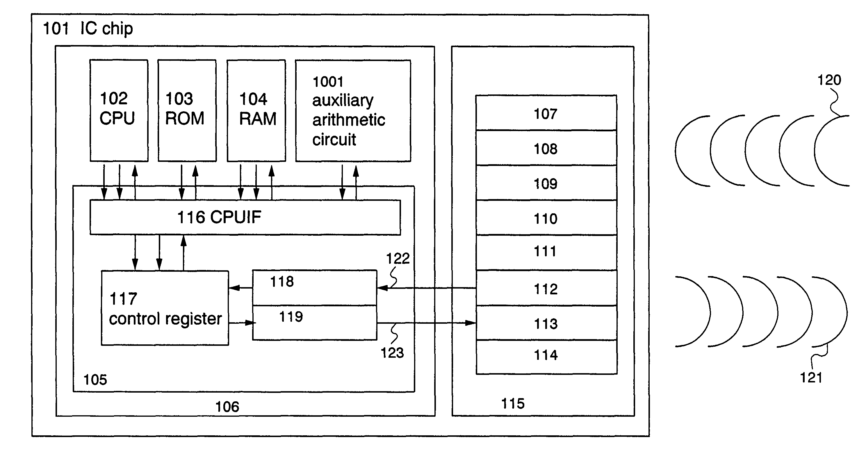
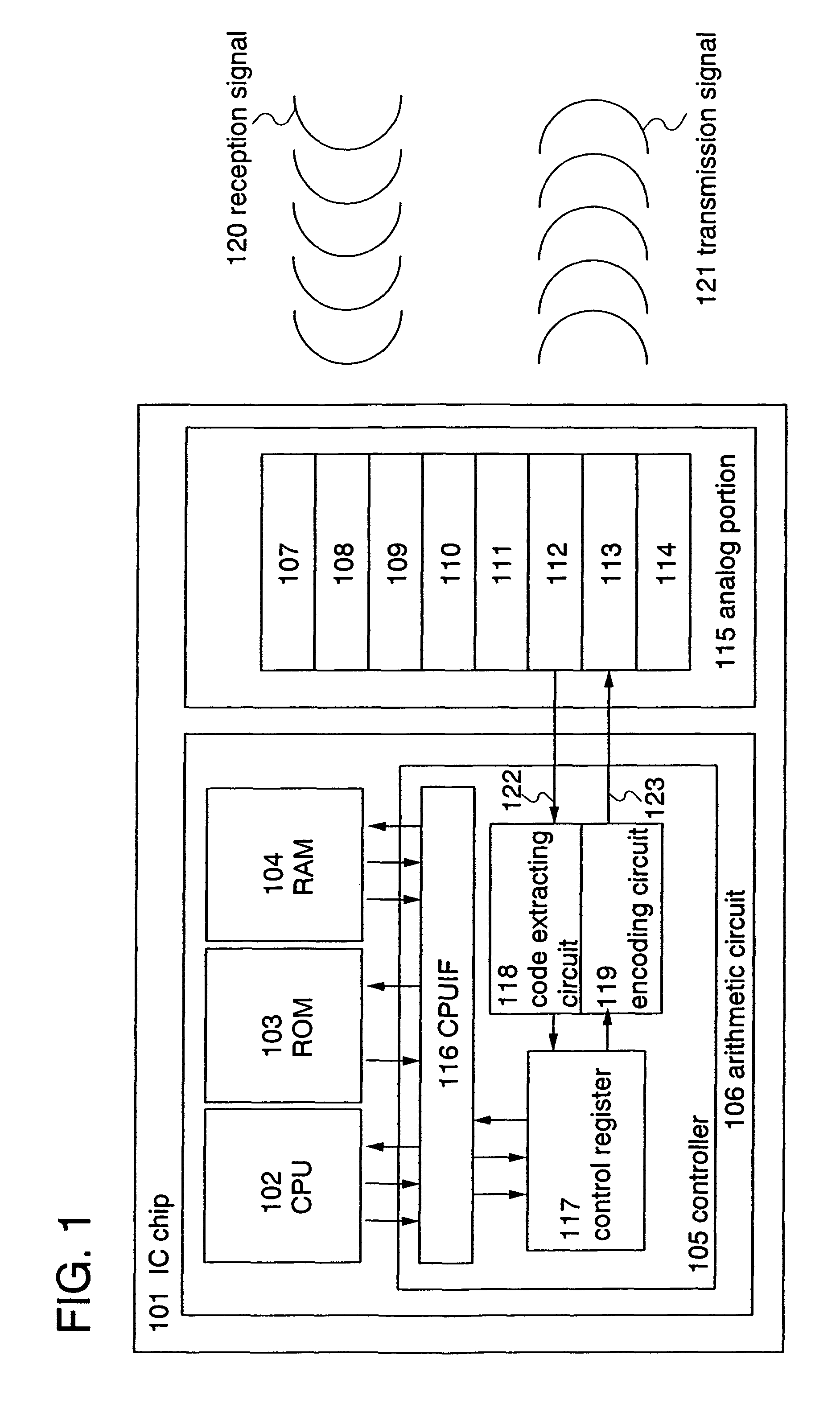
[0044]FIG. 1 shows a block diagram of an IC chip which is to be equipped with an anti-collision function of the present invention.

[0045]In FIG. 1, an IC chip 101 includes an arithmetic circuit 106 and an analog portion 115. The arithmetic circuit 106 includes a CPU (also called a Central Processing Unit) 102, a ROM (also called a Read Only Memory) 103, a RAM (also called a Random Access Memory) 104, and a controller 105. The analog portion 115 includes an antenna 107, a resonant circuit 108, a power supply circuit 109, a reset circuit 110, a clock generating circuit 111, a demodulation circuit 112, a modulation circuit 113, and a power source managing circuit 114. The controller 105 includes a CPU interface (CPUIF) 116, a control register 117, a code extracting circuit 118, and an encoding circuit 119. Note that in FIG. 1, although a re...

embodiment mode 2

[0065]Embodiment Mode 1 shows the structure in which the IC chip can perform the anti-collision function with the anti-collision program, including a plurality of routines to perform the anti-collision function, stored in the ROM. This embodiment mode describes a device configuration and a circuit configuration for realizing an anti-collision function which is different from Embodiment Mode 1. Since a flow chart is similar to that of the embodiment mode, description is made with reference to the drawings described in the embodiment mode if necessary.

[0066]FIG. 10 shows a block diagram of an IC chip which is an object including an anti-collision function of the present invention. FIG. 10 shows a block diagram in which an auxiliary arithmetic circuit 1001 is added to the block diagram of the IC chip of FIG. 1 in Embodiment Mode 1, and which includes, the same as FIG. 1, the arithmetic circuit 106 having the CPU 102, the ROM 103, the RAM 104 and the controller 105, and the analog porti...

embodiment mode 3

[0082]In this embodiment mode, a mode of an IC chip formed by a thin film transistor formed over an insulating substrate is described.

[0083]As shown in FIG. 13A, an insulating substrate 1300 is prepared. A glass substrate, a quartz substrate, a plastic substrate, or the like can be used as the insulating substrate 1300. Further, these substrates can be formed thinner by polishing the back surface thereof or the like. Moreover, a substrate formed by providing a layer using an insulating material over a conductive substrate formed of a metal element or the like or a semiconductor substrate formed of silicon or the like can be used as well. By forming an IC chip over, for example, a plastic substrate, a highly flexible, lightweight, and thin device can be manufactured.

[0084]A peeling layer 1301 is selectively formed over the insulating substrate 1300. Needless to say, the peeling layer 1301 may be formed over the entire surface of the insulating substrate 1300. The peeling layer 1301 i...


PUM


Abstract

An object is to provide a semiconductor device which includes an anti-collision function during or after production of an IC chip just by a change of a program, even when there is a change of a specification of a product accompanying a change of the kind or standard of a signal of a wireless means for each product. A semiconductor device includes an arithmetic circuit and a circuit for transmitting / receiving a signal to / from outside. The arithmetic circuit includes a central processing unit, a random access memory, a read only memory, and a controller. The read only memory stores a program for processing collision avoidance in transmitting / receiving the signal to / from outside. The program is executed in the central processing unit, so that the arithmetic circuit processes collision avoidance.

Description

BACKGROUND OF THE INVENTION[0001]1. Field of the Invention[0002]The present invention relates to a semiconductor device. In particular, the present invention relates to a semiconductor device which transmits / receives a signal to / from outside, a so-called IC chip (also called an ID chip, an IC tag, an ID tag, an RF tag, a wireless tag, an electronic tag, or a transponder) for RFID (Radio Frequency Identification).[0003]Note that a semiconductor device here means that any device which can function by using a semiconductor property.[0004]2. Description of the Related Art[0005]With development of computer technologies and improvement of image recognition technologies, information identification utilizing media such as bar codes has spread widely and been used for identification of product data and the like. It is expected that the amount of information to be identified will further increase in the future. On the other hand, information identification utilizing bar codes is disadvantageo...

Claims


Application Information

Patent Timeline
Patent Type & Authority Patents(United States)
IPC IPC(8): G06F17/00
CPCG06K7/0008G06K7/10029G06K19/0723H01L27/13H01L27/1214H01L27/1266H01L27/092G06K19/07H04B5/00
Inventor DEMBO, HIROKIATSUMI, TOMOAKI
Owner SEMICON ENERGY LAB CO LTD
Why Eureka
Try Eureka