Patterning method using a combination of photolithography and copolymer self-assemblying lithography techniques

a technology of photolithography and self-assembly, which is applied in the direction of photomechanical equipment, instruments, optics, etc., can solve the problems of only printing patterns with 0.93na photolithography tools, and photolithographic techniques can only be used to achieve feature dimensions in the 70-100 nm rang

Active Publication Date: 2011-12-27
INT BUSINESS MASCH CORP
View PDF13 Cites 61 Cited by
  • Summary
  • Abstract
  • Description
  • Claims
  • Application Information

AI Technical Summary

Problems solved by technology

Currently, in the field of lithographic patterning conventional photolithographic techniques can only be used to achieve feature dimensions in the 70-100 nm range.
Unfortunately, this self-assembly copolymer technique is currently not suitable for use in next generation complementary metal oxide semiconductor (CMOS) technology because of the need for precise registration and overlay capabilities.
However, current 0.93NA photolithography tools can only print patterns that can be used to form 100 nm contacts.

Method used


Image

  • Patterning method using a combination of photolithography and copolymer self-assemblying lithography techniques
  • Patterning method using a combination of photolithography and copolymer self-assemblying lithography techniques
  • Patterning method using a combination of photolithography and copolymer self-assemblying lithography techniques

Examples


Embodiment Construction

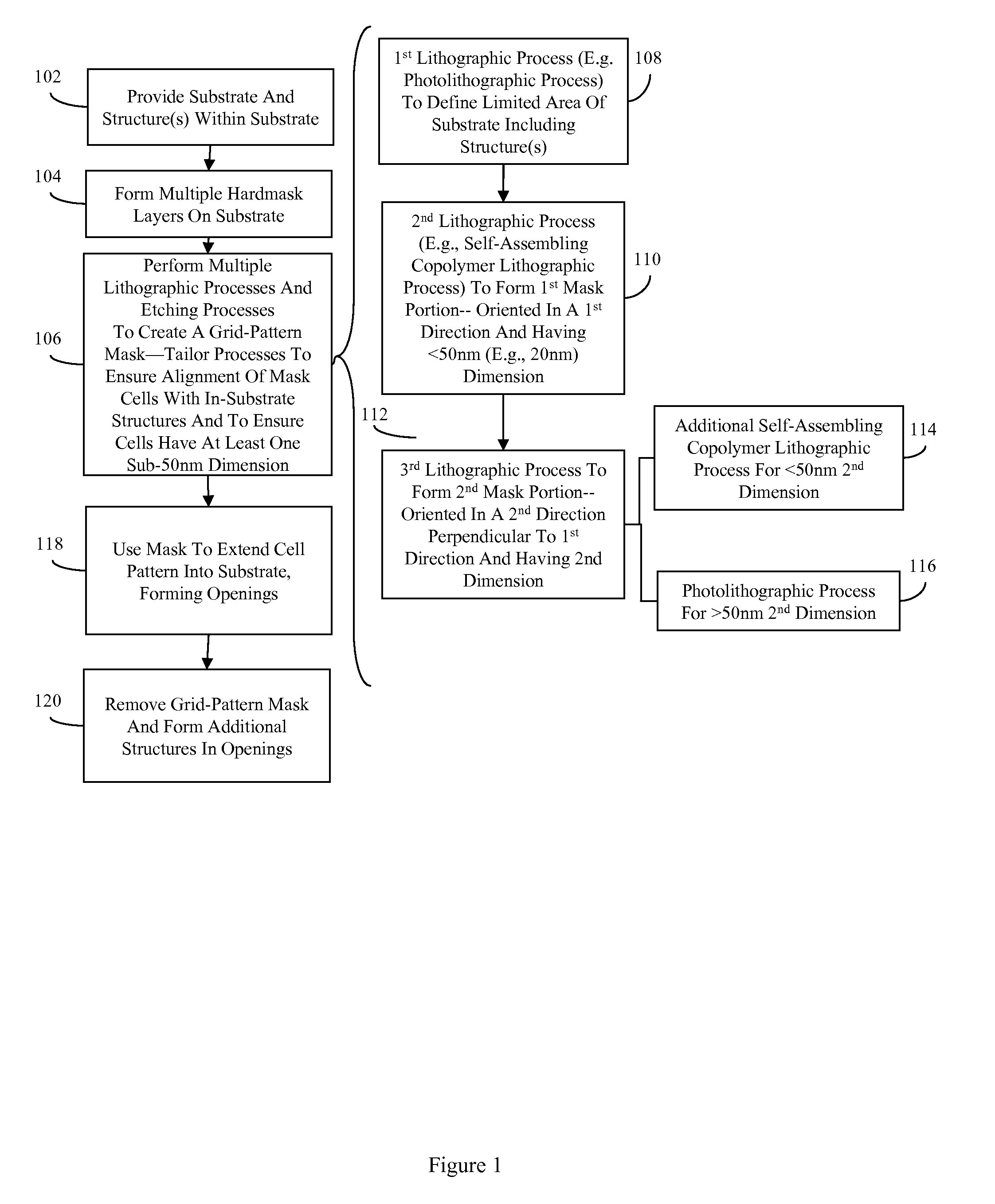
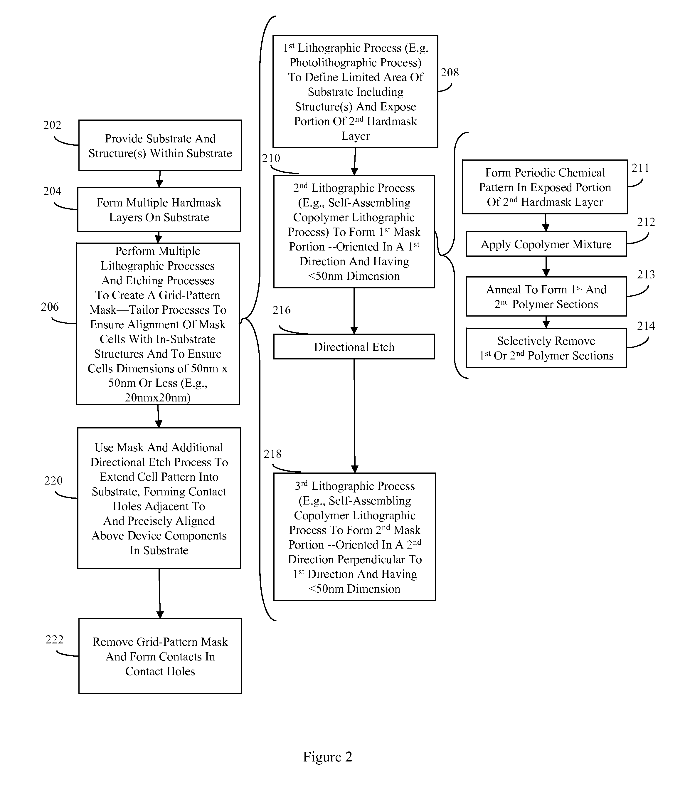
[0049]The embodiments of the invention and the various features and advantageous details thereof are explained more fully with reference to the non-limiting embodiments that are illustrated in the accompanying drawings and detailed in the following description. It should be noted that the features illustrated in the drawings are not necessarily drawn to scale. Descriptions of well-known components and processing techniques are omitted so as to not unnecessarily obscure the embodiments of the invention. The examples used herein are intended merely to facilitate an understanding of ways in which the embodiments of the invention may be practiced and to further enable those of skill in the art to practice the embodiments of the invention. Accordingly, the examples should not be construed as limiting the scope of the embodiments of the invention.

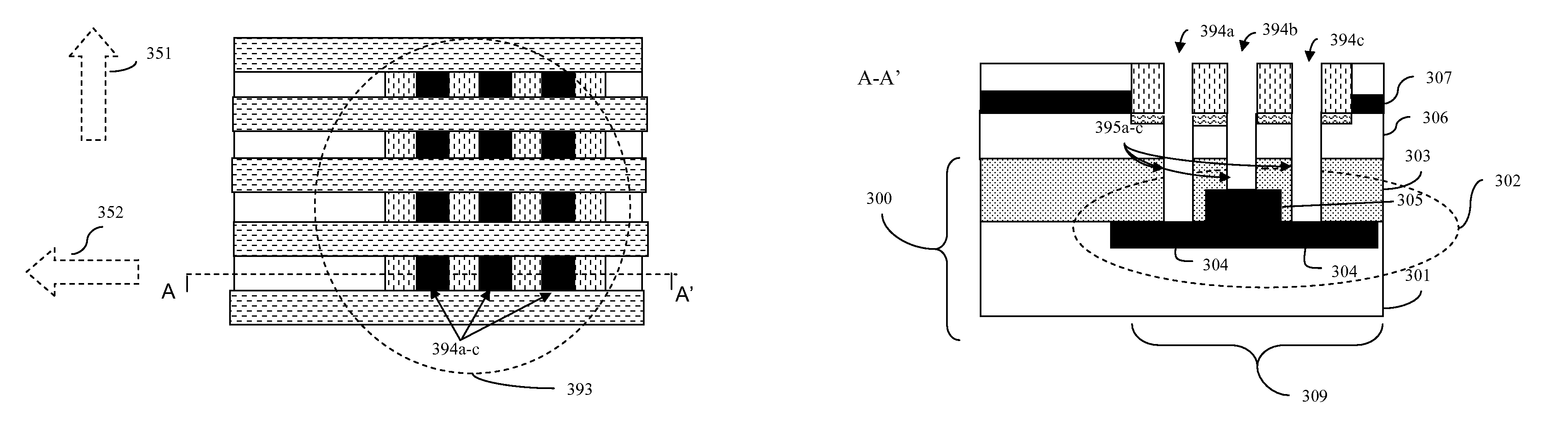
[0050]Device size scaling is an ongoing goal in the semiconductor industry and sub-50 nm feature dimensions are desirable for next generation co...


PUM

PropertyMeasurementUnit
sizesaaaaaaaaaa
cell lengthaaaaaaaaaa

Abstract

Disclosed are embodiments of a lithographic patterning method that incorporates a combination of photolithography and self-assembling copolymer lithography techniques in order to create, on a substrate, a grid-pattern mask having multiple cells, each with at least one sub-50 nm dimension. The combination of different lithographic techniques further allows for precise registration and overlay of the individual grid-pattern cells with corresponding structures within the substrate. The resulting grid-pattern mask can then be used, in conjunction with directional etch and other processes, to extend the cell patterns into the substrate and, thereby form openings, with at least one sub-50 nm dimension, landing on corresponding in-substrate structures. Once the openings are formed, additional structures can be formed within the openings.

Description

BACKGROUND[0001]1. Field of the Invention[0002]The embodiments of the invention generally relate to lithographic patterning of semiconductor wafers and, more particularly, to a method for lithographically patterning semiconductor wafers using a combination of photolithographic and copolymer self-assembling lithographic techniques.[0003]2. Description of the Related Art[0004]Currently, in the field of lithographic patterning conventional photolithographic techniques can only be used to achieve feature dimensions in the 70-100 nm range. To overcome the limitations of conventional photolithographic techniques, self-assembling copolymer lithographic techniques were developed that can be used to form useful periodic patterns with molecular dimensions in the 20-40 nm range (e.g., see “Self-assembling resists for nanolithography” by Nealey et al., Electron Devices Meeting, 2005. IEDM Technical Digest, IEEE International, December 2005 and U.S. Pat. No. 6,746,825 of Nealy et al. issued on J...

Claims


Application Information

Patent Timeline
Patent Type & Authority Patents(United States)
IPC IPC(8): B82Y40/00H01L21/302
CPCH01L21/0273H01L21/0334H01L21/0337G03F7/0035Y10S977/888Y10S977/895Y10S438/947Y10S438/942
Inventor LI, WAI-KINYANG, HAINING S.
Owner INT BUSINESS MASCH CORP
Why Eureka
Try Eureka