
Cache optimizations using multiple threshold voltage transistors

a technology of threshold voltage and transistor, applied in the field of cache optimization, can solve the problems of not meeting the thermal requirements of the integrated circuit, limiting the amount by which the supply voltage can be reduced, and being overly expensive or even infeasible, so as to improve the writeability of the memory, improve the speed of the circuit, and improve the read or write performance of the memory

Active Publication Date: 2012-01-24
APPLE INC
View PDF25 Cites 4 Cited by
  • Summary
  • Abstract
  • Description
  • Claims
  • Application Information

AI Technical Summary

Benefits of technology

The patent text describes a memory circuit that uses lower threshold voltage transistors in its interface circuitry, such as word line drivers and bit line control circuits, to improve memory read and write performance. This may be done by driving the word line driver circuit with signals from a lower voltage domain than the memory circuit, or by using lower threshold voltage transistors in the write data driver circuits to improve writeability over higher threshold voltage transistors in the memory cells. The use of lower threshold voltage transistors may also reduce power and integrated circuit area occupied by the memory circuits.

Problems solved by technology

If power consumption is not managed, meeting the thermal requirements of the integrated circuit (e.g. providing components required to adequately cool the integrated circuit during operation to remain within thermal limits of the integrated circuit) can be overly costly or even infeasible.
However, there are limits to the amount by which the supply voltage can be reduced.
Reducing the supply voltage often reduces the performance of the circuits supplied by that supply voltage.
One limit to the reduction of supply voltage that is experienced in integrated circuits that integrate memories (such as SRAM) is related to the robustness of the memory.
. . i.e. actively conduct current) does not scale well.

Method used


Image

  • Cache optimizations using multiple threshold voltage transistors
  • Cache optimizations using multiple threshold voltage transistors
  • Cache optimizations using multiple threshold voltage transistors

Examples


Embodiment Construction

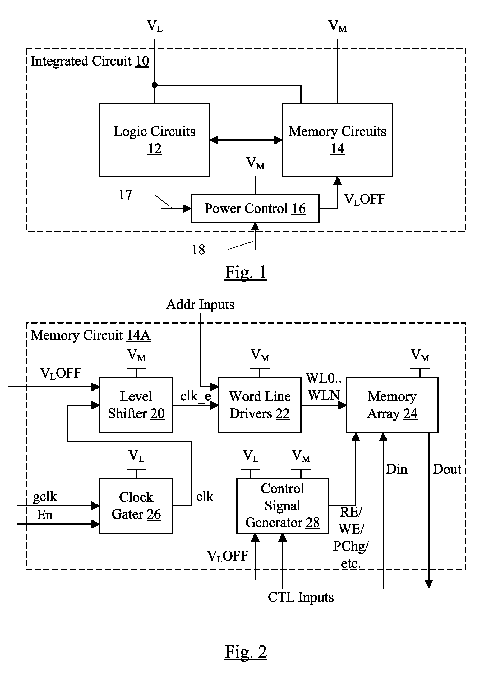
[0018]Turning now to FIG. 1, a block diagram of one embodiment of an integrated circuit 10 is shown. In the illustrated embodiment, the integrated circuit includes one or more logic circuits 12, one or more memory circuits 14, and a power control circuit 16. The logic circuits 12 are coupled to the memory circuits 14. The power control circuit 16 is coupled to the memory circuits 14 (specifically, via a VLOFF signal). The logic circuits 12 are powered by a first supply voltage provided to the integrated circuit 10 (labeled VL in FIG. 1). The memory circuits 14 and the power control circuit 16 are powered by a second power supply voltage provided to the integrated circuit 10 (labeled VM in FIG. 1). In the illustrated embodiment, the memory circuits 14 are also powered by the VL supply voltage, as will be explained in more detail for certain embodiments below. The integrated circuit 10 may generally comprise the logic circuits 12, the memory circuits 14, and the power control circuit ...


PUM


Abstract

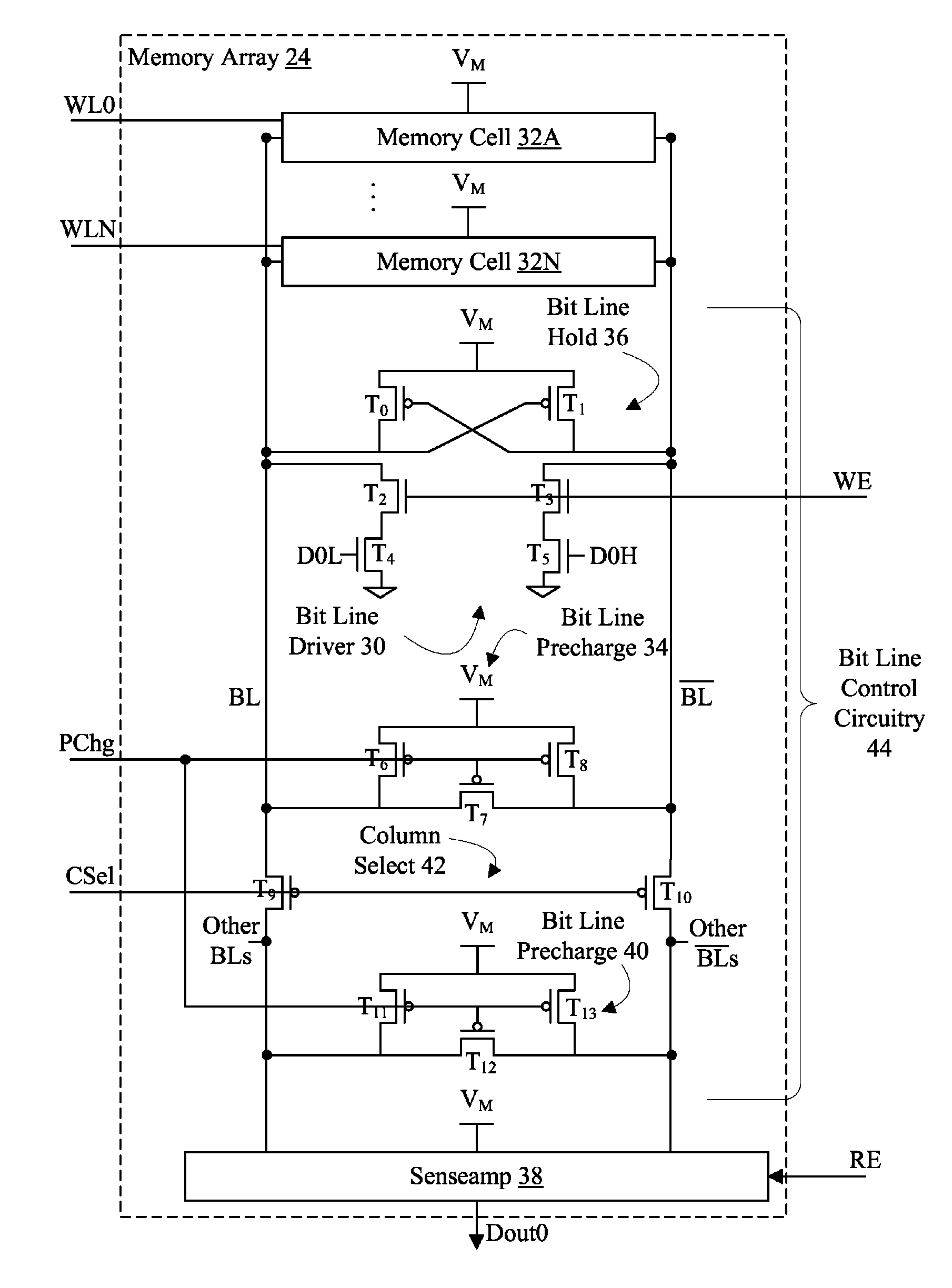
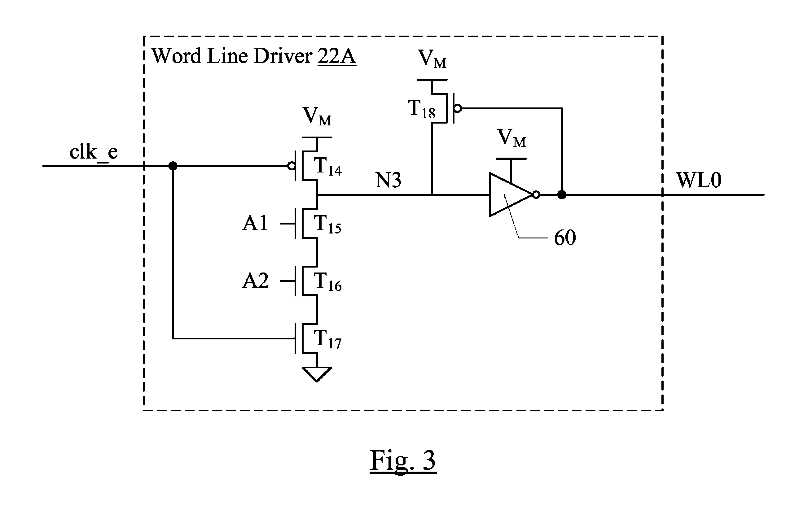
In one embodiment, a memory circuit includes one or more memory cells that include transistors having a first nominal threshold voltage, and interface circuitry such as word line drivers and bit line control circuitry that includes one or more transistors having a second nominal threshold voltage that is lower than the first nominal threshold voltage. For example, the word line driver circuit may be driven by signals from a lower voltage domain than the memory circuit's voltage domain. Lower threshold voltage transistors may be used for those signals, in some embodiments. Similarly, lower threshold voltage transistors may be used in the write data driver circuits. Other bit line control circuits may include lower threshold voltage transistors to permit smaller transistors to be used, which may reduce power and integrated circuit area occupied by the memory circuits.

Description

BACKGROUND[0001]1. Field of the Invention[0002]This invention is related to the field of integrated circuits and, more particularly, to caches in integrated circuits.[0003]2. Description of the Related Art[0004]As the number of transistors included on a single integrated circuitchip” has increased and as the operating frequency of the integrated circuits has increased, the management of power consumed by an integrated circuit has continued to increase in importance. If power consumption is not managed, meeting the thermal requirements of the integrated circuit (e.g. providing components required to adequately cool the integrated circuit during operation to remain within thermal limits of the integrated circuit) can be overly costly or even infeasible. Additionally, in some applications such as battery powered devices, managing power consumption in an integrated circuit can be key to providing acceptable battery life.[0005]Power consumption in an integrated circuit is related to th...

Claims


Application Information

Patent Timeline
Patent Type & Authority Patents(United States)
IPC IPC(8): G11C8/00
CPCG11C7/12G11C8/08G11C11/417
Inventor CAMPBELL, BRIAN J.HESS, GREG M.HUANG, HANG
Owner APPLE INC
Learn More