Logarithmic image sensor with improved dynamic range

a dynamic range and image sensor technology, applied in the field of image sensors, can solve the problems of slow process, low dynamic range of image sensors with conventional integrating pixels, unsuitable for many applications, etc., and achieve the effect of increasing the noise immunity of any analogue signal, reducing the effects of pixel variability and temporal noise, and increasing the amplitud

Inactive Publication Date: 2012-01-31
OXFORD UNIV INNOVATION LTD
View PDF7 Cites 5 Cited by
  • Summary
  • Abstract
  • Description
  • Claims
  • Application Information

AI Technical Summary

Benefits of technology

[0040]The most reliable method of increasing the noise immunity of any analogue signal is to increase its amplitude at the earliest opportunity. In the context of a pixel detector circuit this means designing a circuit with the largest possible output signal range. Furthermore, an ideal pixel circuit should be able to exploit double sampling techniques to reduce the effects of pixel variability and temporal noise in existing linear sensors. This suggests that un...

Problems solved by technology

This causes a problem for image sensors with conventional integrating pixels, which have a linear output of relatively low dynamic range.
However, this is necessarily a slow process, which is unsuitable for many applications (for example, video capture).
In the case of a camera the problem is compounded by the fact that the aim should be to match the performance of the human visual system, which means that the camera should be sensitive to 1% changes in luminance.
However, despite the potentially huge market for a high dynamic range camera, logarithmic cameras remain relatively obscure and undeveloped.
Although this ci...

Method used


Image

  • Logarithmic image sensor with improved dynamic range
  • Logarithmic image sensor with improved dynamic range
  • Logarithmic image sensor with improved dynamic range

Examples


first embodiment

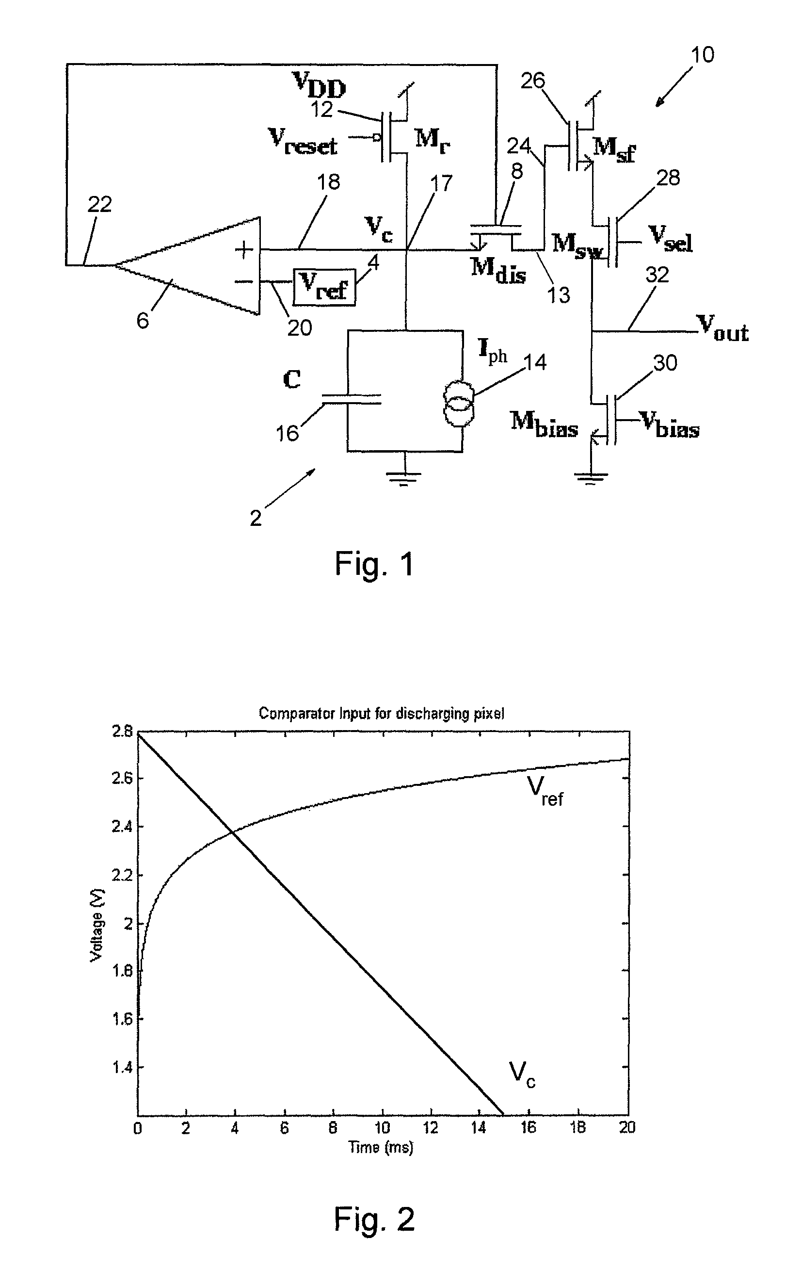
[0051]An image sensor for a camera conventionally includes an array of pixel detectors. FIG. 1 is a schematic circuit diagram of a pixel detector that forms part of such an array in an electronic image sensor according to the invention.

[0052]The pixel detector includes a photosensor device 2, a signal generator 4, comparator 6, a transistor disconnect switch 8, an output device 10 in the form of a read out circuit and a transistor reset switch 12. The comparator 6 and the transistor disconnect switch 8 form a sensing device having an outlet 13 that is connected to the input of the output device 10. In this embodiment, the transistor disconnect switch 8 is an n-channel MOSFET.

[0053]The photosensor device 2 comprises a photodetector 14 connected in parallel with a capacitor 16. The required capacitance C can be provided by a separate capacitor as shown in the drawing and / or by the intrinsic capacitance of other circuit components. The photodetector 14, which is shown here as a constan...

second embodiment

[0067]FIG. 8 is a schematic circuit diagram of a pixel detector that forms part of an electronic image sensor according to the invention. The pixel detector includes a photosensor 102, a first signal generator 104, a sensing device comprising a comparator 106 and a transistor disconnect switch 108, an output device 110 comprising a read out circuit, and a transistor reset switch 112.

[0068]The photosensor 112 comprises a photodetector 114 connected in parallel with a capacitor 116. The photodetector 114 may for example be a photodiode or phototransistor. The photosensor 102 provides a signal at connection 117, represented by the capacitor voltage VC. This photodetector signal is connected to a first input 118 of the comparator 106. The signal generator 104 is connected to a second input 120 of the comparator. The reset switch 112 is also connected to the photosensor 102 through connection 117.

[0069]The comparator 106 has an output 122 for a capture signal, which is connected to the g...

third embodiment

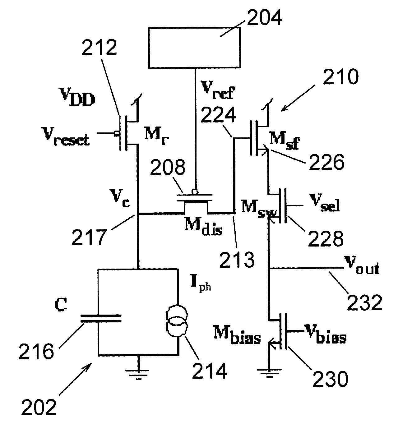
[0076]FIG. 9 is a schematic circuit diagram of a pixel detector according to the invention. This embodiment uses fewer transistors per pixel than the first two embodiments and thus provides significant cost and size advantages over those embodiments. This is particularly important in image sensors with a large number of pixel elements.

[0077]The pixel detector includes a photosensor device 202, a signal generator 204, a sensing device 208 comprising a transistor switch, an output device 210 and a transistor reset switch 212. The transistor switch 208 has an outlet 213 that is connected to the input of the output device 210. In this embodiment, the transistor switch 208 is a p-channel MOSFET, which only conducts when the gate voltage is less than the source voltage by an amount equal to the transistor threshold voltage. When the gate voltage is equal to or greater than the source voltage minus the threshold voltage, the transistor 208 ceases to conduct.

[0078]The photosensor device 202...


PUM


Abstract

An image sensor for an electronic imaging device includes an array of pixel detectors. Each pixel detector includes a photosensor (2) that is constructed and arranged to detect incident light and provide a signal that represents a time integral of the detected light intensity. A signal generator device (4) is constructed and arranged to generate a reference signal that varies according to a predetermined function. A comparator (6) has a first input (18) connected to receive the photosensor signal, a second input (20) connected to receive the reference signal, and an output (22) for providing a capture signal. The comparator (6) is constructed and arranged to generate a capture signal at a time determined by comparing the photosensor signal and the reference signal. A read out device (10) is constructed and arranged to capture a read out signal upon receiving the capture signal. The read out signal represents a logarithm of the integrated detected light intensity.

Description

RELATED APPLICATIONS[0001]This application is the U.S. National Phase filing under 35 U.S.C. §371 of PCT / GB2006 / 003683, filed Oct. 4, 2006, which designated the United States and was published in English, which claims priority under 35 U.S.C. §119(a)-(d) to Great Britain Patent Application No. 0522248.4, filed Nov. 1, 2005. The contents of these applications is incorporated herein by reference in their entireties.FIELD OF THE INVENTION[0002]The present invention relates to an image sensor for an electronic imaging device, and to a method of sensing. The invention also relates to an imaging device having such an image sensor.BACKGROUND OF THE INVENTION[0003]An image sensor for an electronic imaging device such as a camera generally consists of an array of photosensitive picture element detectors (“pixel detectors”). Light falling on the image sensor is detected by the pixel detectors, which generate output signals corresponding to the amount of light falling on each of those detector...

Claims


Application Information

Patent Timeline
IPC IPC(8): H04N5/335H04N3/15
CPCH04N3/155H04N5/35518H04N5/37455H04N25/573H04N25/772H04N3/1556H04N23/73
Inventor COLLINS, STEVE
Owner OXFORD UNIV INNOVATION LTD
Why Eureka
Try Eureka