Illuminating device

a technology of illumination device and light source, which is applied in the direction of lighting and heating apparatus, semiconductor devices for light sources, instruments, etc., can solve the problems of inability to efficiently realize ideal light distribution, high manufacturing cost, and hardly free control of rays, so as to reduce the unevenness of rays

Active Publication Date: 2012-02-21
NALUX CO LTD
View PDF25 Cites 30 Cited by
  • Summary
  • Abstract
  • Description
  • Claims
  • Application Information

AI Technical Summary

Benefits of technology

[0014]Thus, the present invention is based on new findings that a compact illuminating device for illumination at a solid angle of 2π or more can be obtained by appropriately determining a shape of a light exit surface in consideration of paths of light emitted at the first and second points and by appropriately determining a ratio of a size of the optical element in x axis direction to that of the surface light source in x axis direction.
[0052]According to the present embodiment, an illuminating device can be obtained, in which problems of heat from the light source have been solved while reducing unevenness of rays which tends to show up around the boundary between the first light exit surface and the second light exit surface.

Problems solved by technology

However, in this method manufacturing cost is high and there exist problems concerning thermal design of LEDs.
However, there has not existed an optical element by which an ideal light distribution can be efficiently realized.
As a result, incident directions of rays to various positions on the optical surface are not uniform, and therefore the rays can hardly be controlled freely.
Thus, a compact illuminating device in which an optical element is used to distribute light emitted by a surface light source such as an LED to illuminate sufficient amount of light omnidirectionally with solid angles of 2π or more has not been developed.

Method used


Image

  • Illuminating device
  • Illuminating device
  • Illuminating device

Examples


Embodiment Construction

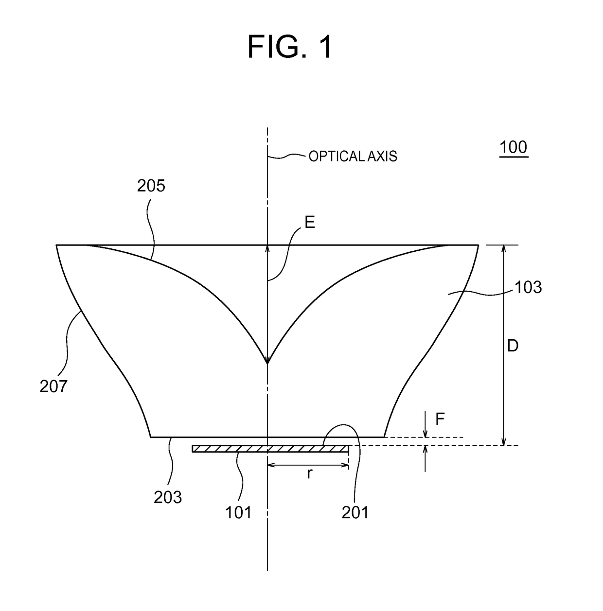
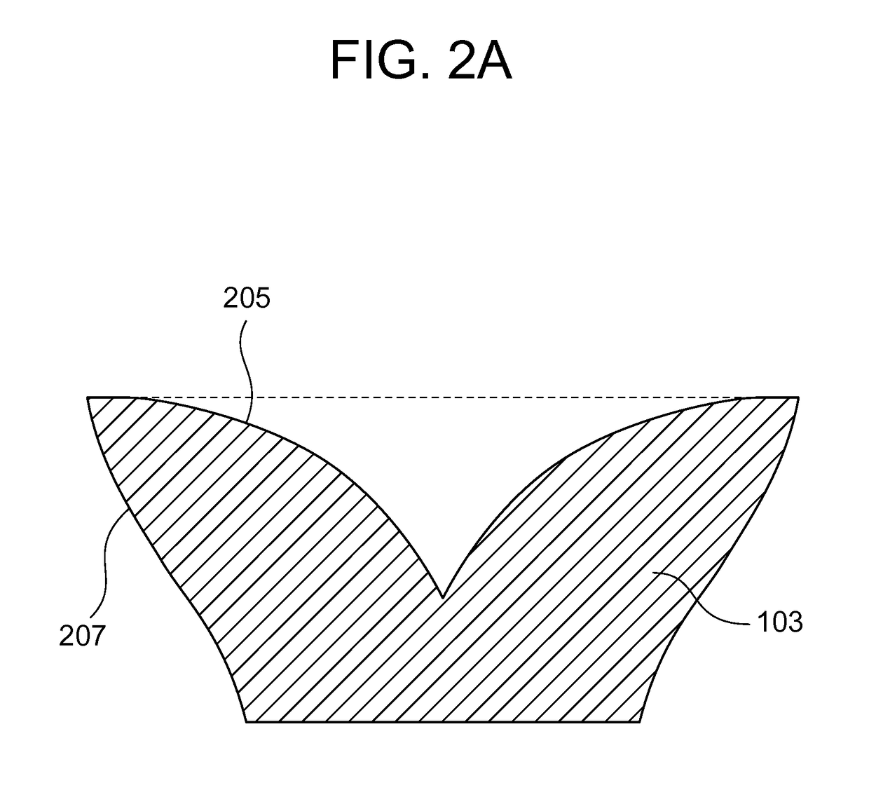
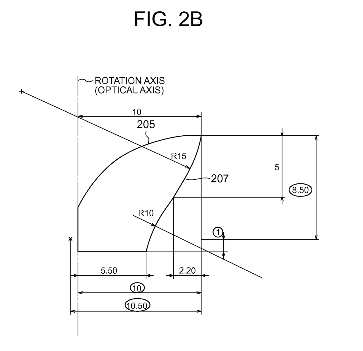
[0090]FIG. 1 shows a configuration of an illuminating device according to an embodiment of the present invention. The illuminating device according to the present embodiment includes a surface light source 101 and an optical element 103. The surface light source 101 may be a single chip of planar LED (Light Emitting Device), planar LED chips arranged on a surface, OLED (Organic Light Emitting Diode) and LEP (Light Emitting Polymer). The surface light source 101 may be circular. When LED chips are arranged on a surface, the surface may have a curvature. Further, the surface light source 101 may be an array of LED chips sealed by a transparent material (for example, silicone resin) of semi-spherical shape. The optical element 103 may have a shape of infinite-fold rotational symmetry around the axis passing through the center of the circle of the surface light source 101 and normal to the surface of the surface light source 101. The axis is referred to as an optical axis.

[0091]A light ...


PUM


Abstract

An illuminating device includes a light source and a light receiving surface, first and second light exit surfaces. When a point at the edge of the light emitting surface is P2 and an axis which passes through a center P1 of a light emitting surface and is perpendicular to the light emitting surface is an optical axis, the optical element has a hollow around the optical axis. The first light exit surface is such that x coordinate of a point most distant from the optical axis on the first light exit surface is at least 1.5 times x coordinate of P2, that in 80% or more of an area in which x coordinate of a point is at least the x coordinate of another point P3, an angle of incidence of light emitted at P1 is at least the critical angle and that in 80% or more of an area in which x coordinate of a point is equal to or smaller than x coordinate of another point P4, an angle of incidence of light emitted at P2 is smaller than the critical angle.

Description

FIELD OF THE INVENTION[0001]The present invention relates to an illuminating device using a surface light source.BACKGROUND ART[0002]Light emitting diodes (LED) have recently been used for illuminating devices as LED light bulbs in place of conventional incandescent light bulbs because of their lower energy consumption. LED light bulbs are required to have a light distribution property similar to that of conventional incandescent light bulbs.[0003]However, blue LED chips have an emitted-light distribution property of close to Lambertian, and therefore a white LED or a bulb-color LED light source using blue LED chips with fluorescent substances also have a light distribution property close to Lambertian. Lambertian means a distribution of emitted light in which intensity of the emitted light is proportional to the cosine of the observation angle. Accordingly, with light sources using LEDs, radiation to areas at the rear of the light source, that is, radiation with a solid angle of 2π...

Claims


Application Information

Patent Timeline
Patent Type & Authority Patents(United States)
IPC IPC(8): F21V17/02
CPCF21V5/04F21V7/0091G02B19/0071G02B19/0028G02B19/0061F21Y2101/02F21Y2105/00F21Y2105/001F21Y2105/10F21Y2115/10H01L33/58
Inventor KANAI, NORIFUMI
Owner NALUX CO LTD
Why Eureka
Try Eureka