Light emitting diode

a diode and light-emitting technology, applied in the direction of basic electric elements, electrical equipment, semiconductor devices, etc., can solve the problems of high cost, insufficient brightness, and difficulty in uniform dispersion and supply of current to the overall led chip from the circular electrode, and achieve the effect of small drive current and high light emission outpu

Inactive Publication Date: 2012-03-20
SUMITOMO CHEM CO LTD
View PDF10 Cites 15 Cited by
  • Summary
  • Abstract
  • Description
  • Claims
  • Application Information

AI Technical Summary

Benefits of technology

[0025]An object of the present invention is to provide a light emitting diode capable of obtaining a high light emission output with a small drive current.

Problems solved by technology

However, in this method, accurate mounting / wiring of several hundred LED chips is necessary to constitute the light source for one illumination, thus requiring much labor in manufacture and incurring higher cost.
However, brightness is not sufficient, if compared with a light bulb or a fluorescent light that are put to practical use as general illumination devices.
However, in order to increase the current that can be flown to the LED, a problem is not limited to the size of the LED chip which needs to be increased, and the following various problems are likely to be generated.
If the LED chip is increased in size, it becomes difficult to uniformly disperse and supply the current to overall LED chip from the circular electrodes.
However, when the large current flows to the branch-shaped wiring electrodes to thereby increase a current density, breakage or deterioration occurs in the wiring electrodes by electromigration.
The deterioration of the wiring electrodes is gradually progressed, thus damaging an advantage of the LEDs such that they have a long service life.
However, when widths of the wiring electrodes are increased to thereby increase the cross-sectional area, emitted lights are blocked by wide wiring electrodes, thus reducing a light extraction efficiency.
However, a formation process of the wiring electrodes becomes difficult and also the wiring electrodes are easily damaged when the LED chips are grasped by a collet, etc.
When the wiring electrodes are damaged, an electric resistance of a damaged part becomes high, and there is a high possibility that the wiring electrodes are broken when the large current flows.
Moreover, a stem side on which the LED chip is mounted, also needs to be formed to withstand the large current, and wiring formed of a thin film such as plating which can be utilized conventionally, can not withstand the large current.
However, in the power source capable of flowing the large current such as 5 A or 10 A, the cost is increased and sufficient insulation measure needs to be secured to prevent a generation of electric leakage.
However, in the technique disclosed by the aforementioned patent documents 1 and 2, although epitaxial layers can be formed on an insulating substrate like 4 elements type LED, the epitaxial layers can not be formed on a transparent substrate.
In a case of simply using a semi-insulating substrate, light emitted from an active layer toward a substrate is absorbed into a surface of the substrate, and therefore high light extraction efficiency can not be realized.
When the air-bridge wiring is made by wire bonding, it requires much labor and a higher cost.
However, in this case, a sufficient cross-sectional area can be hardly obtained in wiring.
When the sufficient cross-sectional area can not be obtained in the wiring, there is a higher risk of breaking the wiring by a stress of resin during resin molding.
Further, in the air-bridge wiring, the wiring is set in a suspended state, and therefore efficient heat diffusion by heat conduction can not be performed, thus raising a temperature of the wiring and easily breaking the wiring due to electromigration.

Method used


Image

  • Light emitting diode
  • Light emitting diode
  • Light emitting diode

Examples


examples

[0078]The light emitting diode having a structure similar to the aforementioned embodiment was manufactured.

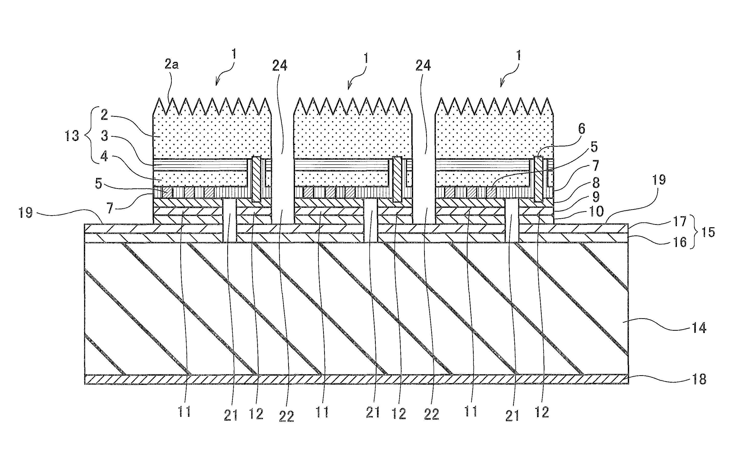
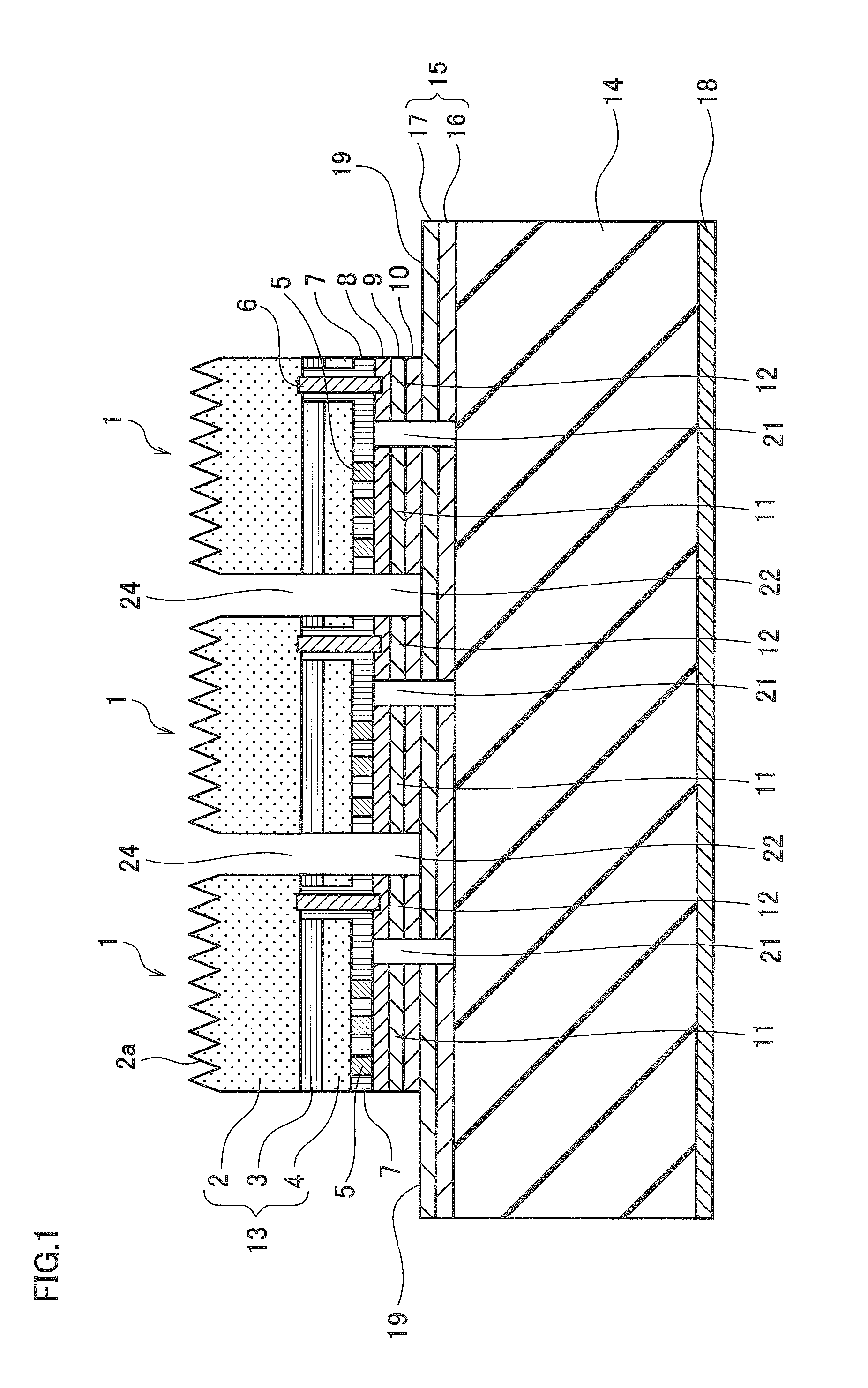
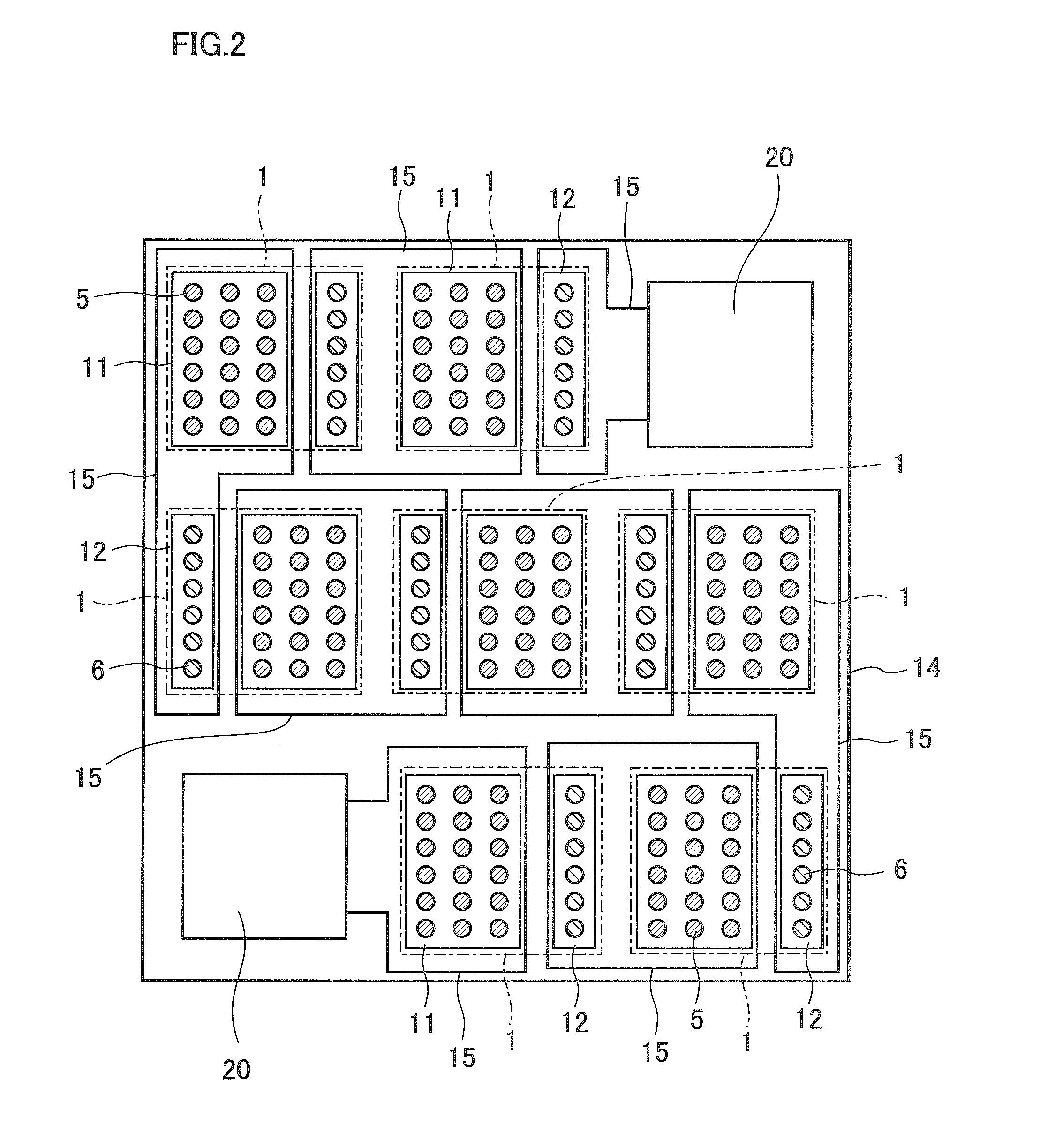
[0079]Dimensions of an outer shape of this light emitting diode were set to 1 mm×1 mm, and about 200 μm (thickness). Further, the outer shape of each light emitting element 1 was set to 320 μm×320 μm. The dimension of the bonding pad electrode 20 was set to 100 μm×100 μm.

(Manufacture of an Epitaxial Wafer for LED with Electrodes)

[0080]As shown in FIG. 3, first, AlGaInP-related epitaxial layers composed of four layers were grown on a substrate 30 composed of n-type GaAs, being an epitaxial growing substrate by MOVPE method, to thereby form an epitaxial wafer for LED. Namely, an etching stop layer 31, the second semiconductor layer 2, being a n-type AlGaInP clad layer, the active layer 3 having a quantum well structure of AlGaInP, and the first semiconductor layer 4, being a p-type AlGaInP clad layer, are sequentially formed on the substrate 30. In order to obtain a further exce...


PUM


Abstract

A light emitting diode is provided, comprising: a substrate; a metal wiring layer disposed on the substrate; alight emitting element provided on the metal wiring layer; wherein the light emitting element comprises: a semiconductor light emitting layer having a first semiconductor layer, an active layer, and a second semiconductor layer formed from the substrate side sequentially; a transparent insulating layer provided on the substrate side of the semiconductor light emitting layer; a first electrode part and a second electrode part provided on the substrate side of the transparent insulating layer in such a manner as being separated from each other, and joined to the metal wiring layer; a first contact part provided so as to pass through the transparent insulating layer and electrically connecting the first electrode part and the first semiconductor layer; and a second contact part provided so as to pass through the transparent insulating layer, the first semiconductor layer, and the active layer, and electrically connecting the second electrode part and the second semiconductor layer.

Description

[0001]The present application is based on Japanese Patent Application No. 2010-067341, filed on Mar. 24, 2010, the entire contents of which are hereby incorporated by reference.BACKGROUND OF THE INVENTION[0002]1. Field of the Invention[0003]The present invention relates to a light emitting diode and further specifically relates to the light emitting diode wherein a light emitting element is provided on a metal wiring layer disposed on a substrate.[0004]2. Description of the Related Art[0005]Light emitting diodes (LEDs) have been used for mainly display, as a center of so-called indicators such as each kind of electronic equipment or measuring gauge.[0006]In recent years, LEDs have a higher light emitting efficiency and there are less fear of heat generation. Therefore, light emission by flowing larger current than before has been enabled. Accordingly, use of the LEDs have been studied as light sources for smaller illumination, and a part of such LEDs is already put to practical use....

Claims


Application Information

Patent Timeline
Patent Type & Authority Patents(United States)
IPC IPC(8): H01L33/22
CPCH01L33/382H01L33/44H01L25/0753H01L27/153H01L33/405Y10S257/918H01L33/62H01L2924/0002H01L2924/00
Inventor UNNO, TSUNEHIRO
Owner SUMITOMO CHEM CO LTD
Why Eureka
Try Eureka