Photodetection circuit

a photodetection circuit and photodiode technology, applied in the field of photodetection circuits, can solve the problems of extremely small voltage drop, the initial impact of the output voltage of the integrating circuit, etc., and achieve the effect of reducing reducing the effect of the parasitic capacitance of the photodiode, and suppressing the oscillation of the outpu

Active Publication Date: 2012-03-27
HAMAMATSU PHOTONICS KK
View PDF17 Cites 21 Cited by
  • Summary
  • Abstract
  • Description
  • Claims
  • Application Information

AI Technical Summary

Benefits of technology

[0008]In this way, in accordance with the above-described photodetecting circuit, it is possible to suppress oscillation of an output while reducing the effect of the parasitic capacitance of the photodiode, and the photodetecting circuit functions as a limiter circuit with respect to an excess current.
[0009]Further, the photodetecting circuit of the present invention includes comparators to which outputs from the integrating circuits are inputted, and a reset signal generating means for resetting the integrating circuits in accordance with an output from the comparators, and the photodetecting circuit performs conversion of a photoelectric current generated in the photodiode into a frequency. That is, when a voltage generated in accordance with a quantity of electric charges stored in the integrating circuit is made higher than a threshold value of the comparator, an output from the comparator is switched. That is, the higher the intensity of the photoelectric current is, the shorter the period in which an output from the comparator is switched is, and when an output from the comparator is switched, the reset signal generating means resets the integrating circuit, and starts charge storage again. In this way, a photoelectric current generated in the photodiode is converted into a frequency.
[0011]According to the photodetecting circuit of the present invention, it is possible to suppress oscillation of an output current, and the photodetecting circuit is capable of functioning as a zero bias circuit in a case of a small photoelectric current, and as a limiter with respect to an excess photoelectric current. The limiter effect with respect to an excess current is furthermore capable of suppressing abnormal operations of the circuit in conjunction therewith.

Problems solved by technology

However, an output voltage in an integrating circuit is originally affected by the parasitic capacitance.
However, this voltage drop is extremely small in a photoelectric current to an extent that a dark current is concerned about, and an electric current due to the positive bias is negligible.

Method used


Image

  • Photodetection circuit
  • Photodetection circuit
  • Photodetection circuit

Examples


Embodiment Construction

[0020]Hereinafter, a photodetecting circuit according to an embodiment will be described. Note that the same elements are denoted by reference numerals, and overlapping descriptions thereof will be omitted.

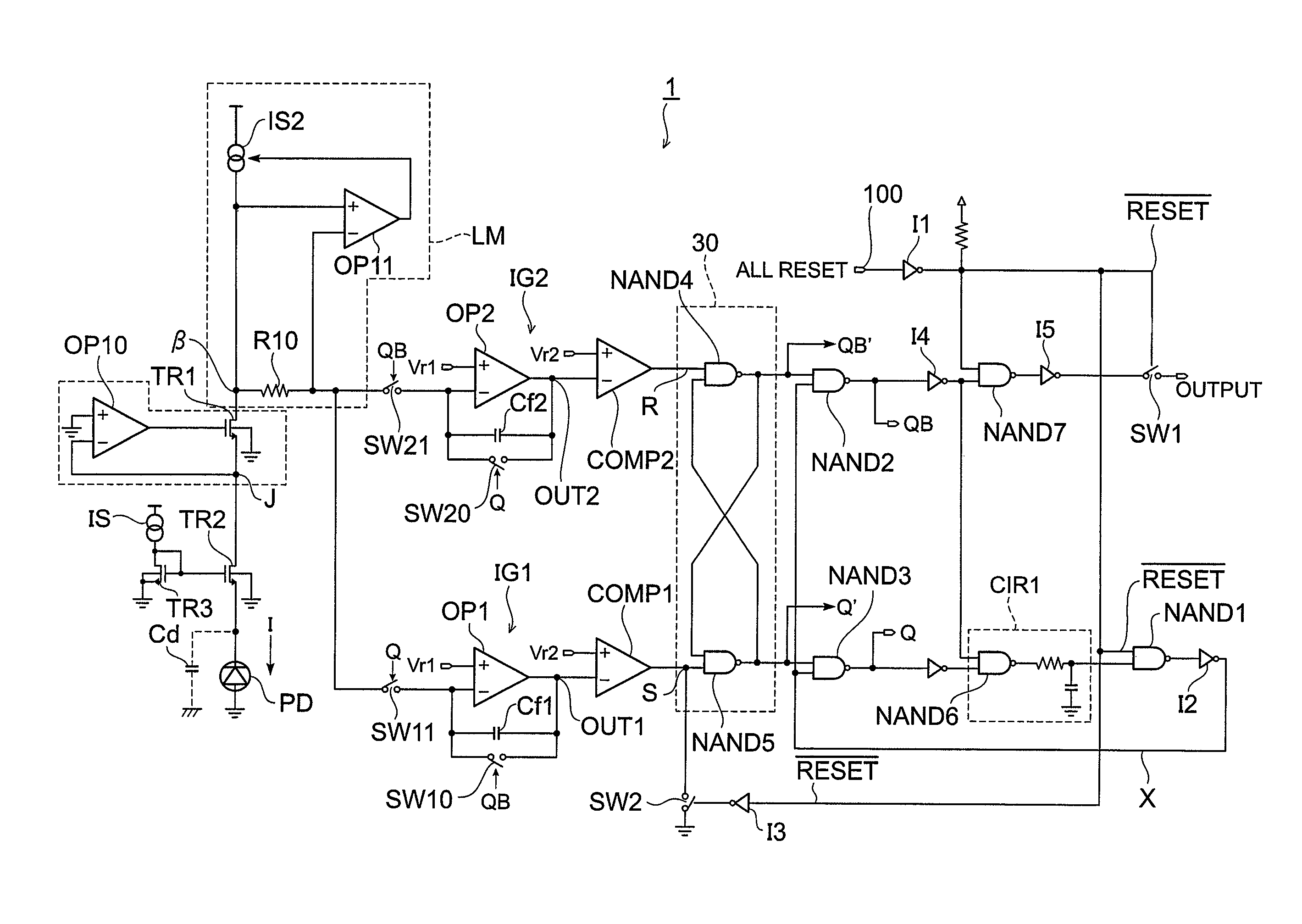
[0021]FIG. 1 is a circuit diagram of the photodetecting circuit.

[0022]The photodetecting circuit 1 includes an integrating circuit IG1 connected to a cathode of a photodiode PD.

[0023]The integrating circuit IG1 has a capacitor Cf1 provided between an output terminal and an inverting input terminal of an operational amplifier OP1, a switch SW10 capable of short-circuiting between the both terminals of the capacitor Cf1, and a gate switch SW11 carrying out connection and disconnection of an input signal with respect to the operational amplifier OP1. A reference potential Vr1 is provided to a non-inverting input terminal of the operational amplifier OP1.

[0024]A signal Q is provided to the gate switch SW11 of the integrating circuit IG1, and when the Q is at an H level, the gate switc...


PUM


Abstract

This photodetecting circuit 1 is capable of suppressing oscillation of an output, and operates as a zero bias circuit in a case of a small photoelectric current to an extent that a dark current is concerned about, and limits an output current in a case of a large photoelectric current to an extent that troubles are caused in the circuit operation. Because a resistive element TR2 is provided in the photodetecting circuit 1, even when a modulation frequency of light, in other words, a frequency of a photoelectric current I flowing in a photodiode PD is made higher, oscillation can be suppressed. Further, due to the resistive element TR2 being inserted, this functions as a limiter as well, and a bias voltage to be applied to the photodiode PD is made to be a positive bias voltage, which prevents an excess current from being generated to suppress abnormal operations of the circuit.

Description

TECHNICAL FIELD[0001]The present invention relates to a photodetecting circuit.BACKGROUND ART[0002]In accordance with a photodetecting circuit described in Patent Document 1, there is disclosed that, in a device loading an electric current generated in a photodiode via an integrating circuit, the photodiode is driven to be zero-biased. When the photodiode is driven to be zero-biased, it is possible to reduce a dark current.Patent Document 1: Japanese Unexamined Patent Application Publication No. 2003-315149[0003]However, in the above-described conventional photodetecting circuit, when light with a high modulation frequency is made incident on the photodiode, an output therefrom oscillates. Further, when intense light such as direct sunlight from the sun is made incident thereon, an excess current is generated in proportion to the light, which may causes troubles in the circuit operation. The present invention has been achieved in consideration of the above-described problems, and an...

Claims


Application Information

Patent Timeline
Patent Type & Authority Patents(United States)
IPC IPC(8): G01J1/44H03F3/08H03F3/14H01J43/00
CPCH04B10/6931H04B10/6911
Inventor SUZUKI
Owner HAMAMATSU PHOTONICS KK
Why Eureka
Try Eureka