Laser apparatus in which surface-emitting semiconductor is excited with semiconduct laser element and high-order oscillation modes are suppressed

a laser element and surface-emitting semiconductor technology, applied in the field of laser elements, can solve the problems of deteriorating laser beam quality, reducing carrier density, and limiting the use of laser beams

Inactive Publication Date: 2003-07-15
NICHIA CORP +1
View PDF4 Cites 32 Cited by
  • Summary
  • Abstract
  • Description
  • Claims
  • Application Information

AI Technical Summary

Benefits of technology

Since the output of the laser apparatus according to the present invention is obtained from the surface-emitting semiconductor element which is excited with laser light emitted from a semiconductor laser element, and the structure for controlling a spatial mode of the second laser light semiconductor laser element is provided, instability of the spatial mode due to the thermal lens effect or the plasma effect can be effectively suppressed. Therefore, it is possible to stably maintain a fundamental transverse mode in a wide output range from low power to high power (in particular, in the high output power region), and obtain high-quality laser light in the fundamental transverse mode.
(i) The above structure may have a size which is 0.1 to 10 times as large as a diameter to which the second laser light spreads at a position of the structure for controlling the spatial mode of the second laser light. In this case, the characteristics and beam shape of the output of the laser apparatus are particularly improved.
(ii) The structure may be realized by a pinhole spatial filter being arranged at a light exit end surface of the surface-emitting semiconductor element, having a pinhole, and allowing passage of the second laser light emitted by the surface-emitting semiconductor element, through only the pinhole. In this case, it is possible to increase resonator loss in high-order modes than that in the fundamental mode. Therefore, the oscillation in the high-order modes can be effectively suppressed, and resultantly oscillation in the fundamental transverse mode is realized.
(iv) The second mirror may have a limited area, be arranged in parallel with a light exit end surface of the surface-emitting semiconductor element, and realize the above structure for controlling the spatial mode of the second laser light. Since the laser light in the fundamental transverse mode can be selectively reflected by the second mirror, it is possible to increase resonator loss in high-order modes more than that in the fundamental mode. Therefore, the oscillation in the high-order modes can be effectively suppressed, and resultantly oscillation in the fundamental transverse mode is realized.

Problems solved by technology

Conventionally, narrow-stripe single-transverse-mode semiconductor laser devices, which emit high quality laser beams, have a drawback that the practical output power is at most about 200 to 300 mW.
That is, since the rate of carrier supply for generating laser light is limited by the carrier diffusion process when the output power is high, carrier density decreases in a region where the laser beam intensity is high.
Thus, the quality of the laser beams deteriorates, and kinks are produced in the current-light output characteristics.
The second cause for the above drawback is the great optical output density.
Therefore, heavy load is imposed on the semiconductor medium, and various characteristics of the semiconductor laser device deteriorate.
Thus, it is difficult to obtain a reliable narrow-stripe single-transverse-mode semiconductor laser device which emits laser light with high output power.
However, these techniques are approaching their limits.
However, the structure and process are complicated.
In addition, the above semiconductor laser devices are sensitive to temperature distribution, and the spatial oscillation mode is unstable.
The spatial mode becomes further unstable when output power is high, since a cavity is generated in a carrier distribution due to generation of laser light having high output power (i.e., spatial hole burning occurs), and refractive indexes decrease with increase in the number of carriers due to the so-called plasma effect.
However, in this semiconductor laser device, it is difficult to emit laser light with high output power in a single transverse mode.
As described above, it is very difficult to achieve a single transverse mode oscillation with high output power in the conventional semiconductor laser devices.
On the other hand, in the conventional semiconductor-laser excited solid-state laser apparatuses, it is difficult to achieve high speed modulation of laser light by directly modulating semiconductor laser elements which are provided as excitation light sources since the lifetimes of fluorescence emitted from rare earth elements which constitute solid-state laser crystals are very long.

Method used


Image

  • Laser apparatus in which surface-emitting semiconductor is excited with semiconduct laser element and high-order oscillation modes are suppressed
  • Laser apparatus in which surface-emitting semiconductor is excited with semiconduct laser element and high-order oscillation modes are suppressed
  • Laser apparatus in which surface-emitting semiconductor is excited with semiconduct laser element and high-order oscillation modes are suppressed

Examples


first embodiment

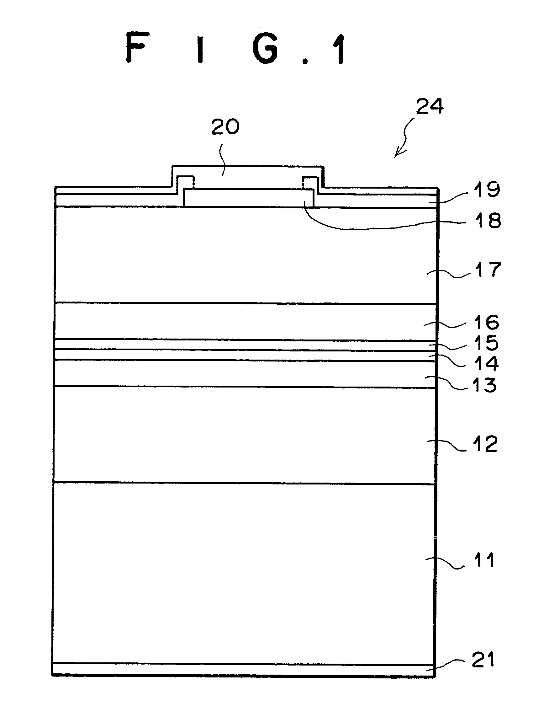
The semiconductor laser element which emits laser light in the 810 nm band is used as an excitation light source in the first embodiment. FIG. 1 is a crosssectional view of the semiconductor laser. The semiconductor laser element used as the excitation light source in the first embodiment is produced as follows.

Initially, an n-type GaAs buffer layer 12, an n-type Al.sub.0.63 Ga.sub.0.37 As cladding layer 13, an n-type or i-type (intrinsic) InGaP optical waveguide layer 14, an InGaAsP single-quantum-well active layer 15, a p-type or i-type InGaP optical waveguide layer 16, a p-type Al.sub.0.63 Ga.sub.0.37 As cladding layer 17, a p-type GaAs cap layer 18 are formed on an n-type GaAs (001) substrate 11 by organometallic vapor phase epitaxy. Thereafter, areas of the p-type GaAs cap layer 18 other than a stripe area having a width of 100 .mu.m and corresponding to an oscillation stripe are removed by etching using an ammonia etchant, and then a SiO.sub.2 insulation film 19 is formed. Nex...

second embodiment

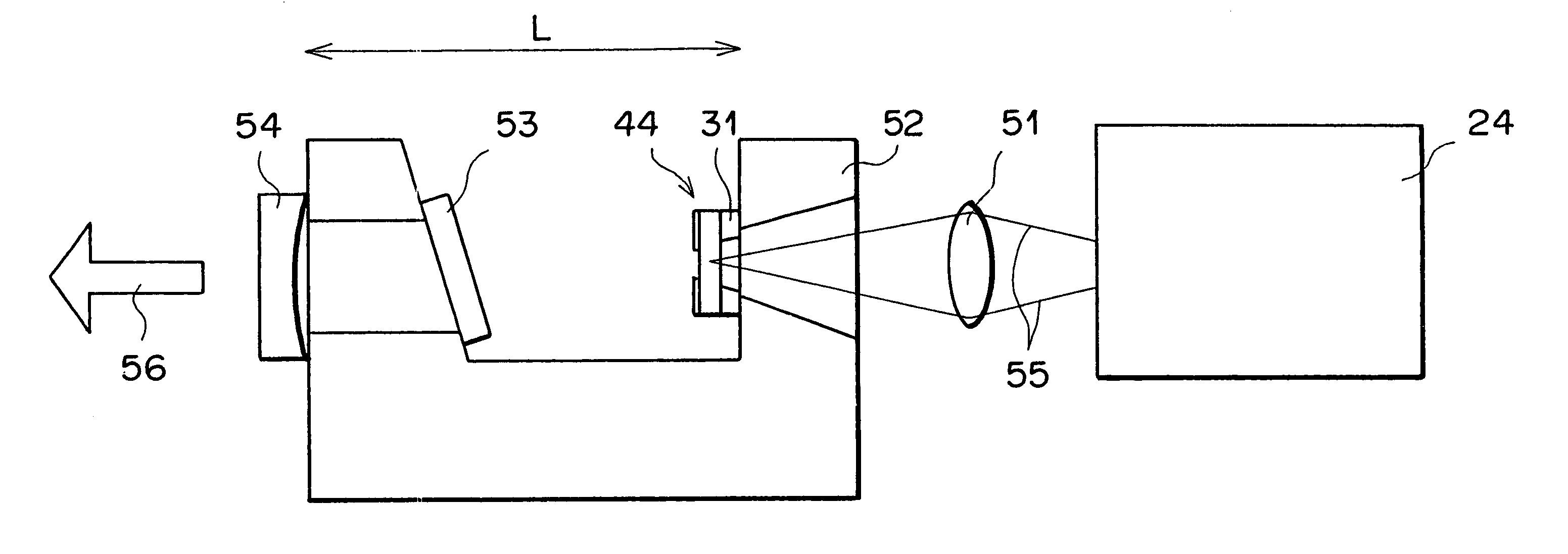
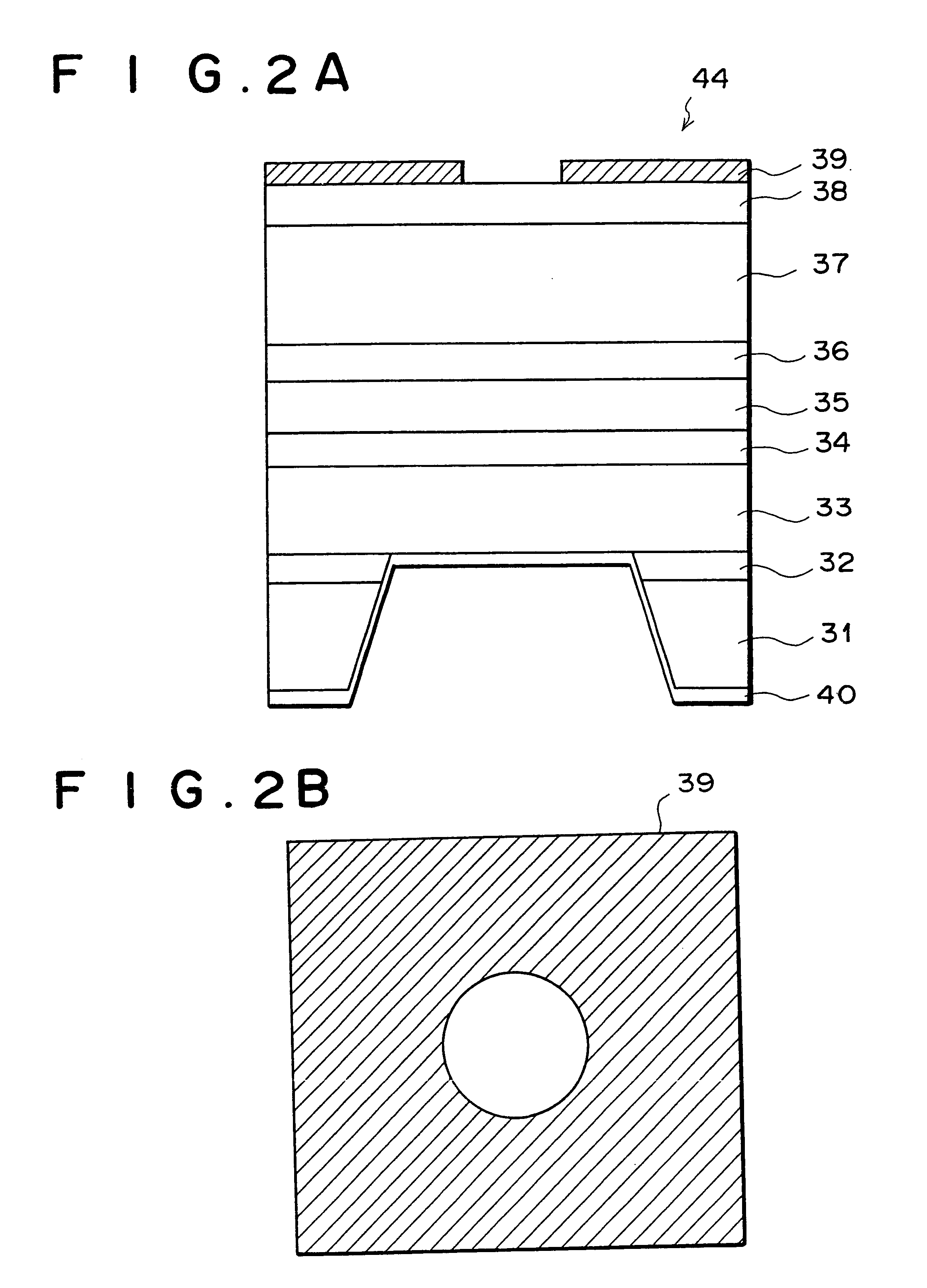
FIG. 4 is a crosssectional view of a surface-emitting semiconductor element which is used in the laser apparatus as the second embodiment of the present invention. The surface-emitting semiconductor element of FIG. 4 is excited with excitation laser light emitted from the semiconductor laser element 24 of FIG. 1, and oscillates at the wavelength of 980 nm. The surface-emitting semiconductor element used in the second embodiment is produced as follows.

Initially, a GaAs buffer layer 62, a Bragg reflection mirror 63, a GaAs optical confinement layer 64, and a GaAs / In.sub.0.2 Ga.sub.0.8 As multiple-quantum-well active layer 65 are formed on a GaAs (001) substrate 61 in the first process of organometallic vapor phase epitaxy. The Bragg reflection mirror 63 is comprised of twenty pairs of GaAs and Al.sub.0.7 Ga.sub.0.3 As layers, the GaAs layer in each pair has a thickness of .lambda. / 4n.sub.GaAs, the Al.sub.0.7 Ga.sub.0.3 As layer in each pair has a thickness of .lambda. / 4n.sub.Al0.7Ga0....

third embodiment

The semiconductor laser element which emits laser light in the 370 nm band is used as an excitation light source in the third embodiment. FIG. 6 is a crosssectional view of the semiconductor laser. The semiconductor laser element used as the excitation light source in the third embodiment is produced as follows.

Initially, an n-type GaN (0001) substrate 91 is formed in accordance with the method disclosed by Nakamura et al., "InGaN / GaN / AlGaN-Based Laser Diodes Grown on GaAs Substrate with a Fundamental Transverse Mode", Japanese Journal of Applied Physics Part 2 Letters, vol. 37, 1998, pp. L1020. Then, an n-type Ga.sub.1-z1 Al.sub.z1 N / GaN superlattice cladding layer 92 (0z2>0), a Ga.sub.1-z4 Al.sub.z4 N (doped with Si) / In.sub.x0 Ga.sub.1-x0 N multiple-quantum-well active layer 94 (z4>0, x0.gtoreq.0), a p-type Ga.sub.1-z3 Al.sub.z3 N carrier confinement layer 95 (0.35>z3>z2), a p-type or i-type Ga.sub.1-z2 Al.sub.z2 N optical waveguide layer 96, a p-type Ga.sub.1-z1 Al.sub.z1 N / GaN s...


PUM


Abstract

A laser apparatus includes a semiconductor laser element, a surface-emitting semiconductor element including a first mirror, and a second mirror. The semiconductor laser element emits first laser light having a first wavelength. The surface-emitting semiconductor element is excited with the first laser light, and emits second laser light having a second wavelength which is longer than the first wavelength. The first mirror in the surface-emitting semiconductor element is arranged on one side of the first active layer. The second mirror is arranged outside the surface-emitting semiconductor element so that the first and second mirrors form a resonator in which the second laser light resonates. The surface-emitting semiconductor element includes a structure for controlling a spatial mode of the second laser light.

Description

1. Field of the InventionThe present invention relates to a laser apparatus using a semiconductor laser element.2. Description of the Related ArtConventionally, narrow-stripe single-transverse-mode semiconductor laser devices, which emit high quality laser beams, have a drawback that the practical output power is at most about 200 to 300 mW. There are two causes for this drawback. The first cause is so-called spatial hole burning. That is, since the rate of carrier supply for generating laser light is limited by the carrier diffusion process when the output power is high, carrier density decreases in a region where the laser beam intensity is high. Due to spatial hole burning, the refractive index of the semiconductor medium increases, and the waveguide mode is affected by the increase in the refractive index. Thus, the quality of the laser beams deteriorates, and kinks are produced in the current-light output characteristics. The second cause for the above drawback is the great opt...

Claims


Application Information

Patent Timeline
Patent Type & Authority Patents(United States)
IPC IPC(8): H01S5/183H01S5/04H01S5/00H01S5/14H01S5/022
CPCB82Y20/00H01S5/041H01S5/141H01S5/18308H01S3/1062H01S5/0207H01S5/0213H01S5/02248H01S5/3432H01S5/34333H01S2301/166H01S5/02325
Inventor HAYAKAWA, TOSHIRO
Owner NICHIA CORP
Why Eureka
Try Eureka