Laser diode and method of manufacture

a technology of laser diodes and diodes, applied in the direction of laser details, laser cooling arrangements, semiconductor lasers, etc., can solve the problems of reducing the maximum output power that can be achieved, reducing the life of the device, and limiting the maximum output power. achieve the effect of suppressing the emission of high-order transverse optical modes

Inactive Publication Date: 2005-12-01
FIRECOMMS
View PDF7 Cites 32 Cited by
  • Summary
  • Abstract
  • Description
  • Claims
  • Application Information

AI Technical Summary

Benefits of technology

[0002] The single longitudinal mode operation, low threshold current, and narrow output beam of vertical cavity surface emitting lasers (VCSELs) has ensured that VCSELs are increasingly being deployed in applications such as data transmission in optical networks, optical interconnects, optical storage, sensing, display and laser printing.
[0003] For many of these applications it is also highly desirable that the VCSEL not only operate in a single longitudinal mode but that the VCSEL also operate in a fundamental transverse mode. Such VCSELs show increased modulation bandwidth, narrow spectrum, reduced noise, improved coupling efficiency to single mode fibre and whose output beam can be focused to a small ‘well-behaved’ Gaussian spot which is often a requirement for many sensing and display applications.
[0005] A method of achieving fundamental transverse mode operation for a VCSEL is to implement a selectively oxidised current aperture [1] within the laser structure whereby the mode is confined through strong index confinement between the Al2O3 and semiconductor material. To achieve fundamental transverse operation the radius of the current aperture must be kept in the region of only a few microns, and typically for a 850 nm VCSEL the aperture would be in the region of 4 μm. Although the operation of fundamental transverse mode VCSELs has been demonstrated using this method it is nevertheless the case that such VCSELs are prone to a number of significant drawbacks. In particular, small selectively oxidised aperture VCSELs show large differential resistance, which is not conducive with high-speed modulation, and high current densities which may lead to reduced device life-times. The small aperture also limits the maximum output power that can be achieved while still maintaining a fundamental transverse mode. At high drive currents the VCSELs also tend to support multiple transverse modes as thermal lensing effects and gain spatial hole burning begin to predominate.
[0006] A technique to enable the use of a large diameter current confinement layer while still maintaining fundamental operation has been put forward [2] based on the use of multiple oxidation layers (mode suppression layers) positioned immediately above the current confinement layer that suppress the oscillation of higher order modes. The function of these mode suppression layers is to increase the scattering losses experienced by the higher order modes and have an aperture larger than the current confinement layer. Although the results shown in Ref [2] show promise the device uses an excessive number of thick mode suppression layers in the vicinity of the active region to achieve sufficient scattering loss to suppress the higher order modes. As the wet selective oxidation process causes an increase in in-built stress within the device, the use of a several thick selective oxidation layers close to the active region is not to be recommended as it is likely to reduce the reliability of the device. The VCSEL embodiments revealed here both avoid this problem and allow an increased level of manufacturing control in relation to achieving the desired diameters of the various oxide apertures.
[0023] In another embodiment, an oxide layer of optical path length of approximately 1 / 4 λ thickness is deposited and patterned on the surface of the VCSEL such that an annular oxide structure is realised whose function is to suppress the emission of high order transverse optical modes.

Problems solved by technology

Although the operation of fundamental transverse mode VCSELs has been demonstrated using this method it is nevertheless the case that such VCSELs are prone to a number of significant drawbacks.
In particular, small selectively oxidised aperture VCSELs show large differential resistance, which is not conducive with high-speed modulation, and high current densities which may lead to reduced device life-times. The small aperture also limits the maximum output power that can be achieved while still maintaining a fundamental transverse mode.
As the wet selective oxidation process causes an increase in in-built stress within the device, the use of a several thick selective oxidation layers close to the active region is not to be recommended as it is likely to reduce the reliability of the device.

Method used


Image

  • Laser diode and method of manufacture
  • Laser diode and method of manufacture
  • Laser diode and method of manufacture

Examples


Embodiment Construction

[0032] The invention will be more clearly understood from the following description of some embodiments thereof, given by way of example only with reference to the accompanying drawings in which:—

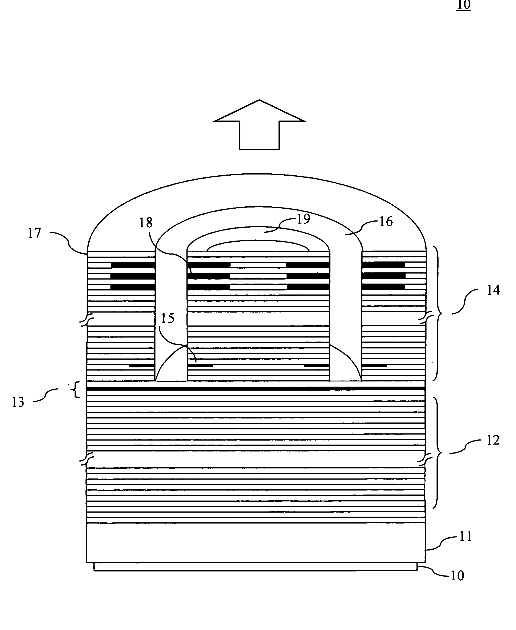
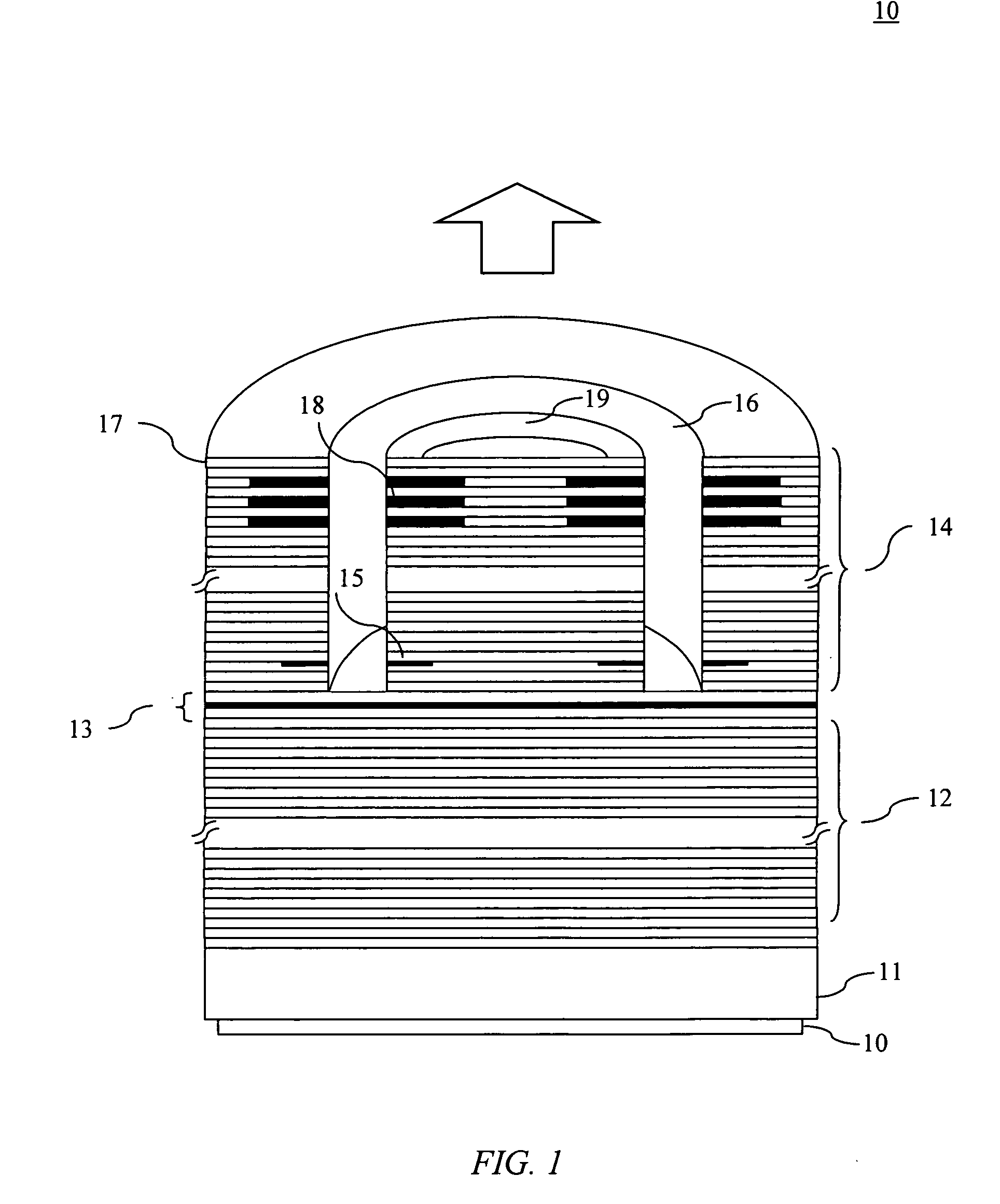
[0033]FIG. 1 is a diagrammatic cross-sectional view of a VCSEL diode of the invention;

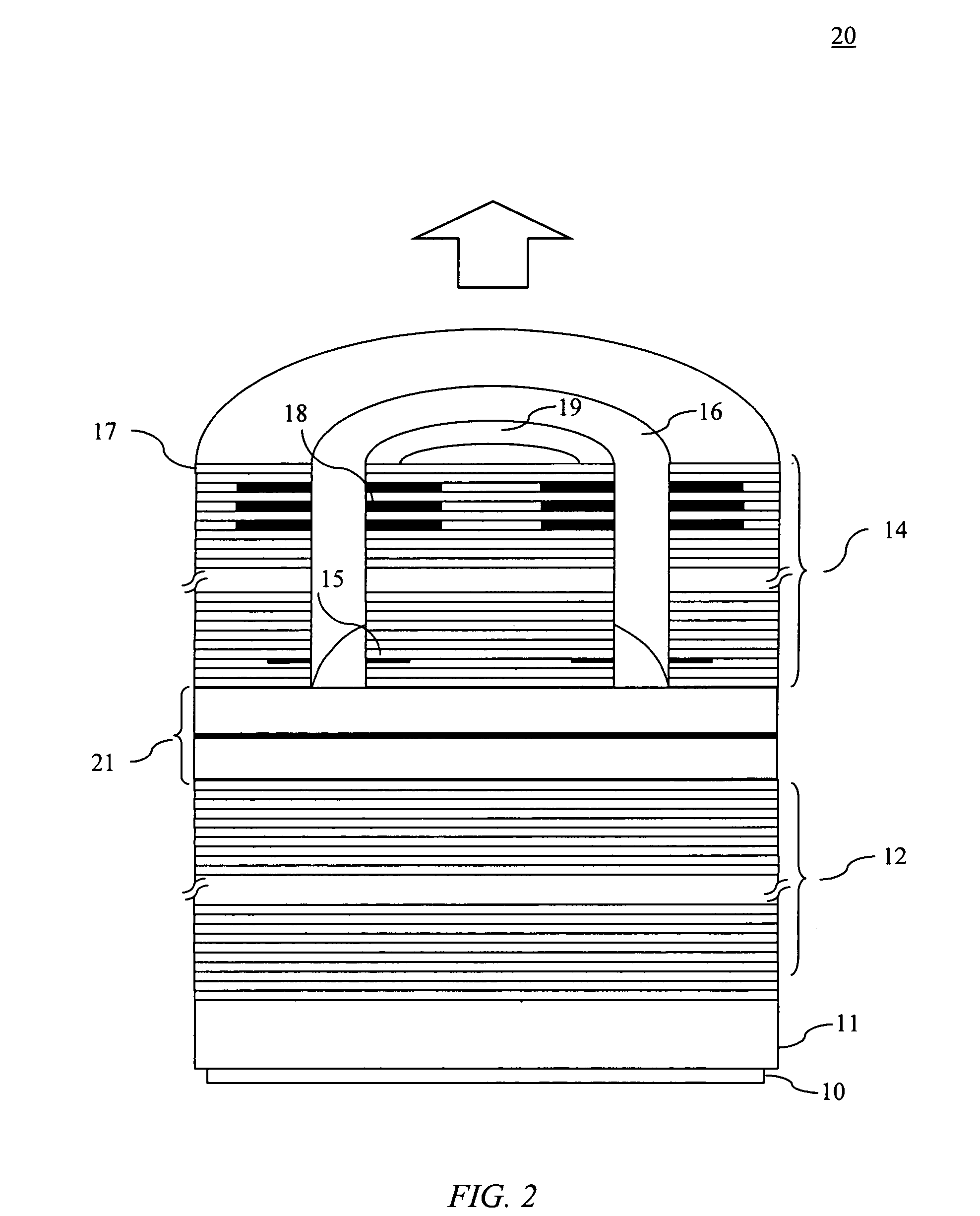
[0034]FIG. 2 is diagrammatic cross-sectional view of another embodiment of the VCSEL diode in which mode control selective oxidation layers are used in conjunction with a multiple wavelength active region cavity.

[0035]FIG. 3 is a diagrammatic cross-sectional view of the VCSEL diode when fabricated using a multi-step etch and oxidation process; and

[0036]FIG. 4 is diagrammatic cross-sectional view of another embodiment of the VCSEL diode in which an oxide mode control is implemented on the surface of the VCSEL.

[0037] Referring to FIG. 1, a general schematic representation of a VCSEL diode 10 of the invention is shown. The VCSEL comprises a bottom electrode 10, conducting substrate material 11, a bottom m...


PUM


Abstract

VCSEL diode comprises a bottom electrode (10), conducting substrate material (11), a bottom mirror (12) formed by a multilayer distributed Bragg reflector (DBR) of certain conductivity and reflectivity RA, and an active region (13) comprising a plurality of layers some of which are quantum wells. It also comprises a top mirror (14) formed by a multilayer distributed Bragg reflector (DBR) with reflectivity RB<RA and conductivity of a second type. There are a number of layers (15, 18) which through a process of selective oxidation (exposure to a high temperature wet atmosphere) may be selectively converted to oxide layers, therefore producing well defined internal oxide apertures within the top mirror. There is a high-conductivity semiconductor top contact layer (17), a top electrode layer (19) with a centrally located aperture from which light is emitted, and a trench (16) which defines a mesa type VCSEL. The VCSEL comprises at least one oxide suppression layer in the top mirror whose function it is to suppress high order transverse optical modes.

Description

[0001] The invention relates to laser diodes and to their manufacture. [0002] The single longitudinal mode operation, low threshold current, and narrow output beam of vertical cavity surface emitting lasers (VCSELs) has ensured that VCSELs are increasingly being deployed in applications such as data transmission in optical networks, optical interconnects, optical storage, sensing, display and laser printing. [0003] For many of these applications it is also highly desirable that the VCSEL not only operate in a single longitudinal mode but that the VCSEL also operate in a fundamental transverse mode. Such VCSELs show increased modulation bandwidth, narrow spectrum, reduced noise, improved coupling efficiency to single mode fibre and whose output beam can be focused to a small ‘well-behaved’ Gaussian spot which is often a requirement for many sensing and display applications. [0004] In both scanning and holographic storage applications it is necessary that the VCSELs operate in a funda...

Claims


Application Information

Patent Timeline
Patent Type & Authority Applications(United States)
IPC IPC(8): H01S3/098H01S5/183H01S5/343
CPCB82Y20/00H01S5/18313H01S5/18333H01S2301/166H01S5/34326H01S5/3436H01S5/18358
Inventor LAMBKIN, JOHN DOUGLAS
Owner FIRECOMMS
Why Eureka
Try Eureka