Integrated circuit inductors with reduced magnetic coupling

a technology of integrated circuits and inductors, applied in the field of electrical, electronic and computer arts, can solve the problems of inductors that can couple magnetically, create unwanted interference signals, and simulate inductors that exhibit high parasitic effects, and achieve the effects of reducing coupling, isolation, and thus performan

Active Publication Date: 2012-03-27
BELL SEMICON LLC
View PDF4 Cites 0 Cited by
  • Summary
  • Abstract
  • Description
  • Claims
  • Application Information

AI Technical Summary

Benefits of technology

[0007]Embodiments of the present invention meet the above-noted need by providing techniques for fainting IC inductors having directional electromagnetic emission so as to reduce magnetic coupling between such inductors when placed in close relative proximity to one another. By reducing the coupling between adjacent IC inductors, isolation, and hence performance, between multi-channel circuits, including, for example, LC oscillators, as well as other circuits and applications employing IC inductors, can be beneficially improved. Moreover, such reduced coupling between adjacent IC inductors can be achieved, in accordance with aspects of the present invention, without the need to increase physical spacing between the inductors, thereby reducing the required area and corresponding cost of the IC.

Problems solved by technology

Unfortunately, simulated inductor circuits frequently exhibit high parasitic effects, and often generate significantly more noise than circuits constructed using discrete inductors, and are therefore undesirable.
In some applications, such as, for example, SERDES (serializer / deserializer) and integrated radios, if there are two transmit and / or receive channels operating at slightly different frequencies (e.g., 400 parts-per-million (ppm) apart), then the inductors can couple magnetically and create unwanted interference signals.
Moreover, spiral inductors take up a disproportionately large share of the available surface area on an IC substrate.
These methods, however, only reduce electric field interfere and not magnetic coupling, which is a primary source of coupling between spiral inductors.

Method used


Image

  • Integrated circuit inductors with reduced magnetic coupling
  • Integrated circuit inductors with reduced magnetic coupling
  • Integrated circuit inductors with reduced magnetic coupling

Examples


Embodiment Construction

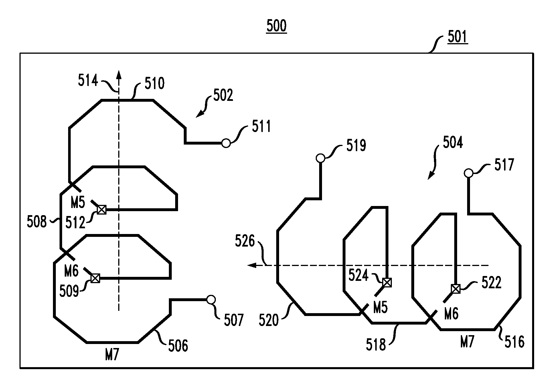
[0018]The present invention will be described herein in the context of exemplary IC inductor structures. It is to be understood, however, that the techniques of the present invention are not limited to the IC inductor structures shown and described herein. Rather, embodiments of the invention are directed broadly to techniques for reducing magnetic coupling between two or more IC inductors when placed in close relative proximity to one another. Although preferred embodiments of the invention may be fabricated in a silicon wafer, embodiments of the invention can alternatively be fabricated in wafers comprising other materials, including but not limited to gallium arsenide (GaAs), indium phosphide (InP), etc.

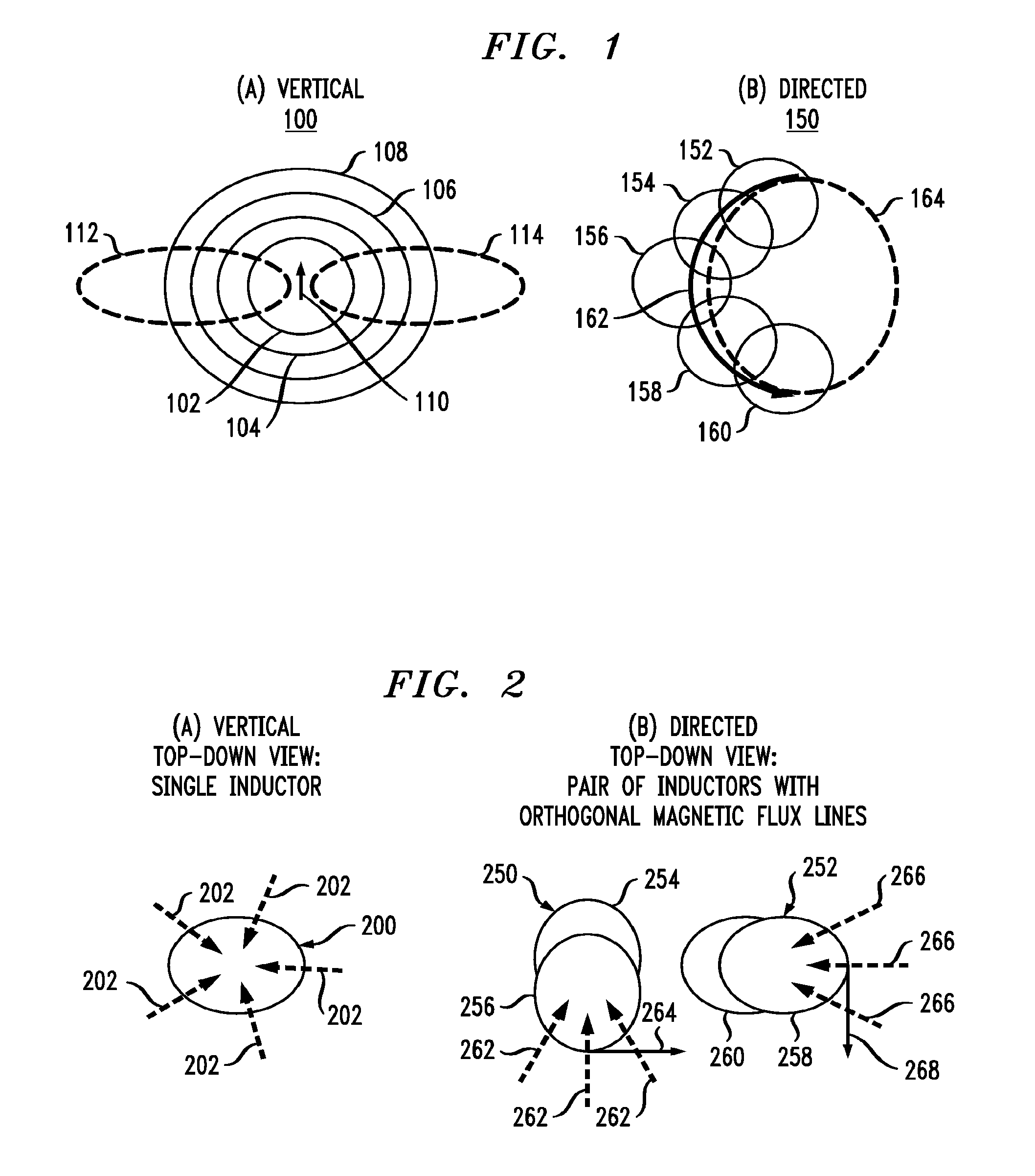
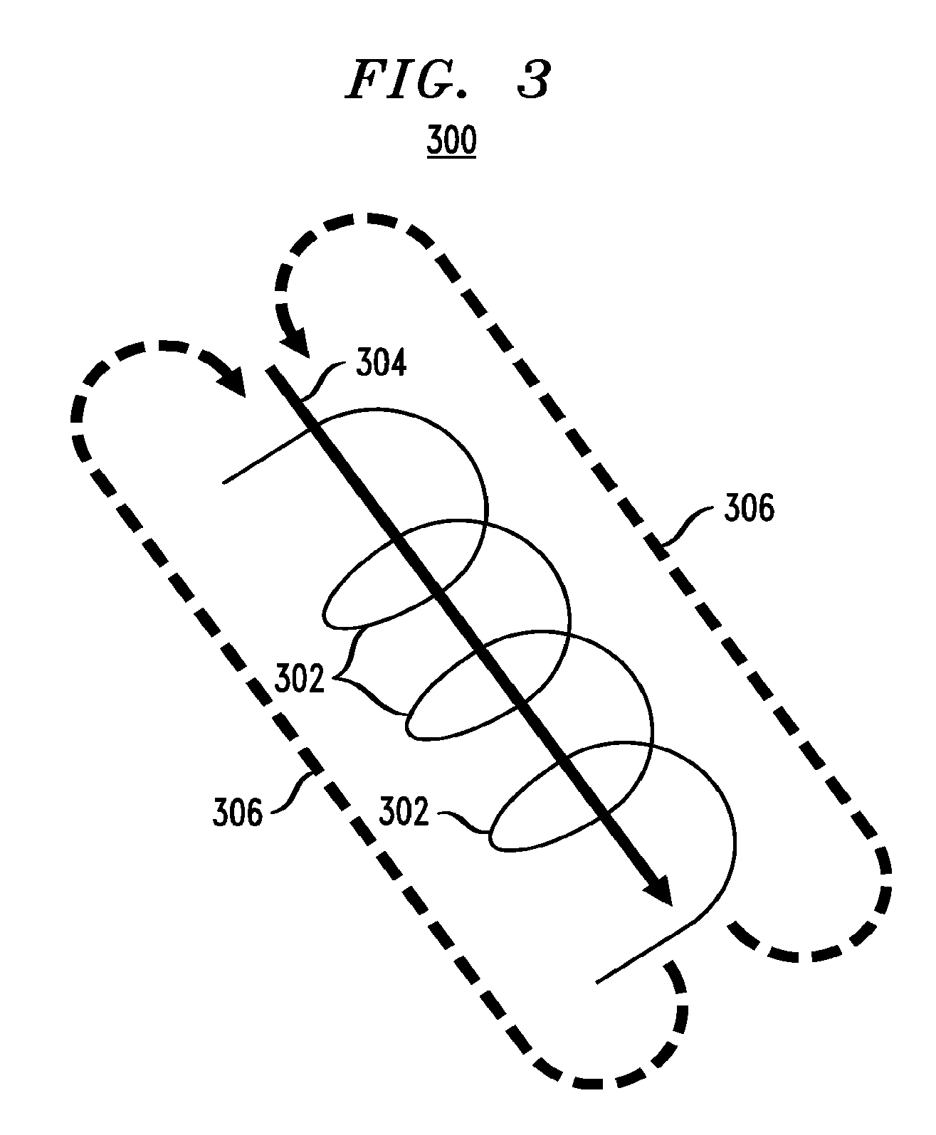
[0019]FIGS. 1A and 1B are conceptual views of an illustrative spiral inductor 100 and an exemplary directed inductor 150, respectively, according to an embodiment of the present invention. With reference to FIG. 1A, a top plan view of the illustrative spiral inductor 100 is shown....


PUM


Abstract

An IC inductor structure is provided which includes a first inductor element formed on a semiconductor substrate and at least a second inductor element formed on the semiconductor substrate proximate the first inductor element. The first inductor element has a first effective magnetic field direction associated therewith, and the second inductor element has a second effective magnetic field direction associated therewith. The first and second inductor elements are oriented relative to one another so as to create a non-zero angle between the first and second effective magnetic field directions.

Description

FIELD OF THE INVENTION[0001]The present invention relates generally to the electrical, electronic, and computer arts, and more particularly relates to integrated circuit (IC) inductors.BACKGROUND OF THE INVENTION[0002]Inductors are used in a wide range of applications, including, for example, communication systems, signal processing systems, filters, tank circuits, etc. As these electronic systems have become more integrated and scaled down, effectively, systems on a chip (SOC), circuit designers have sought to eliminate the use of large auxiliary components, such as inductors. When unable to eliminate inductors in their designs, engineers have sought to reduce the size of the inductors they do utilize so as to facilitate the inclusion of such inductors on-chip.[0003]One approach to integrating inductors on-chip is to employ simulated inductors rather than discrete inductors. Simulating inductors using active circuits, which are easily miniaturized, is one approach to eliminating th...

Claims


Application Information

Patent Timeline
Patent Type & Authority Patents(United States)
IPC IPC(8): H01L27/08
CPCH01L23/5227H01L2924/0002H01L2924/00
Inventor MAO, WEIWEIMOINIAN, SHAHRIARPAIST, KENNETH WADEWILSON, WILLIAM B.
Owner BELL SEMICON LLC
Why Eureka
Try Eureka