Optical element and exposure apparatus
a technology applied in the field of optical elements and exposure apparatuses, can solve the problems of failure to obtain a desired optical performance, and achieve the effect of preventing the deterioration of the sealing member
- Summary
- Abstract
- Description
- Claims
- Application Information
AI Technical Summary
Benefits of technology
Problems solved by technology
Method used
Image
Examples
embodiment 1
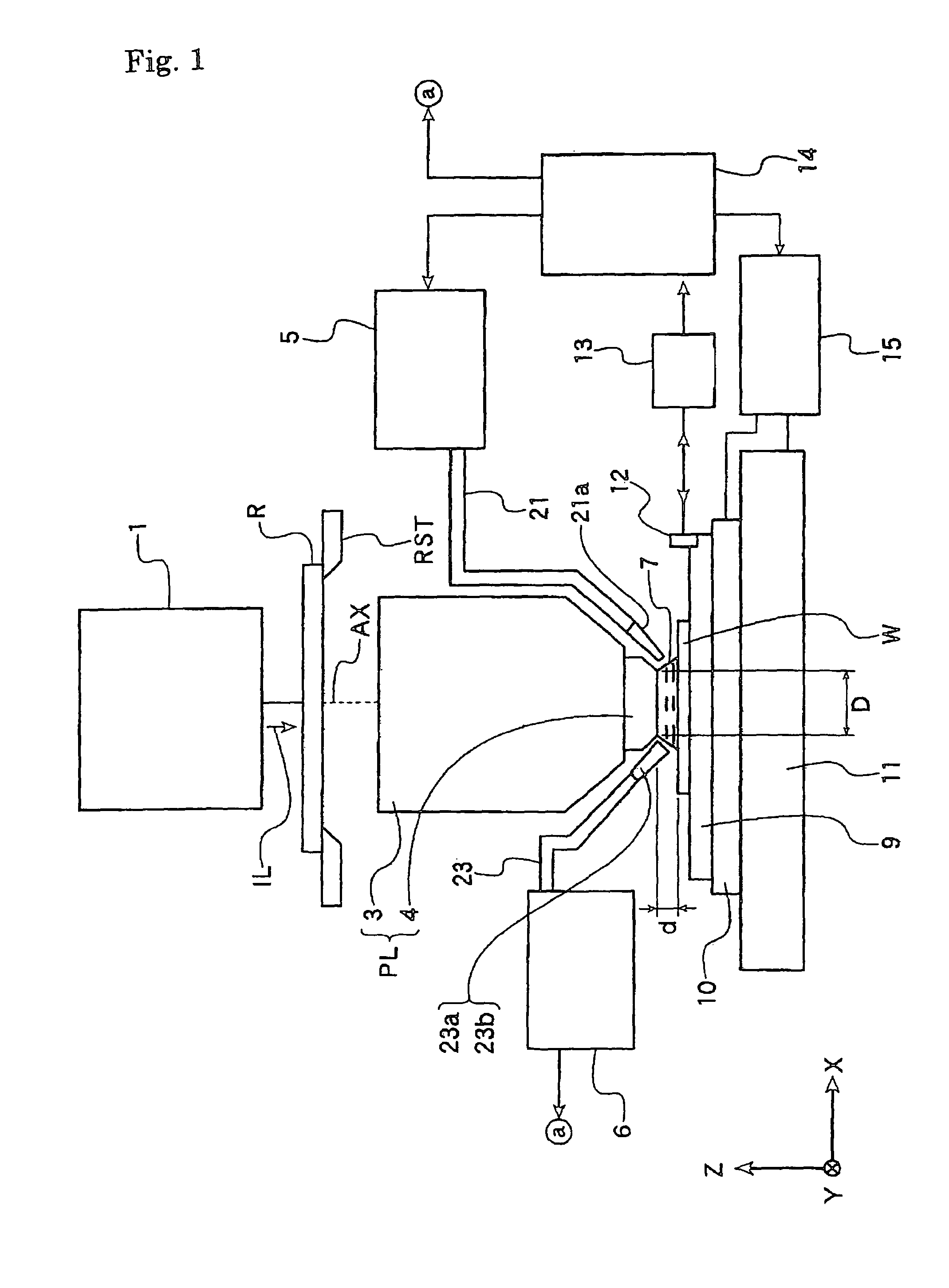
[0181]A projection exposure apparatus according to Embodiment 1 of this invention will now be described with reference to the accompanying drawings. FIG. 1 is a view showing a schematic configuration of a projection exposure apparatus applying the step and repeat method according to Embodiment 1. It is to be noted that an XYZ orthogonal coordinate system as illustrated in FIG. 1 will be set up in the following explanation, and positional relations of respective members will be described with reference to this XYZ orthogonal coordinate system. In terms of the XYZ orthogonal coordinate system, an X axis and a Y axis are set parallel to a wafer W while a Z axis is set in the orthogonal direction to the wafer W. In terms of the XYZ orthogonal coordinate system in the figure, an XY plane is actually set to a parallel plane to a horizontal plane while the Z axis is set in the vertical direction.
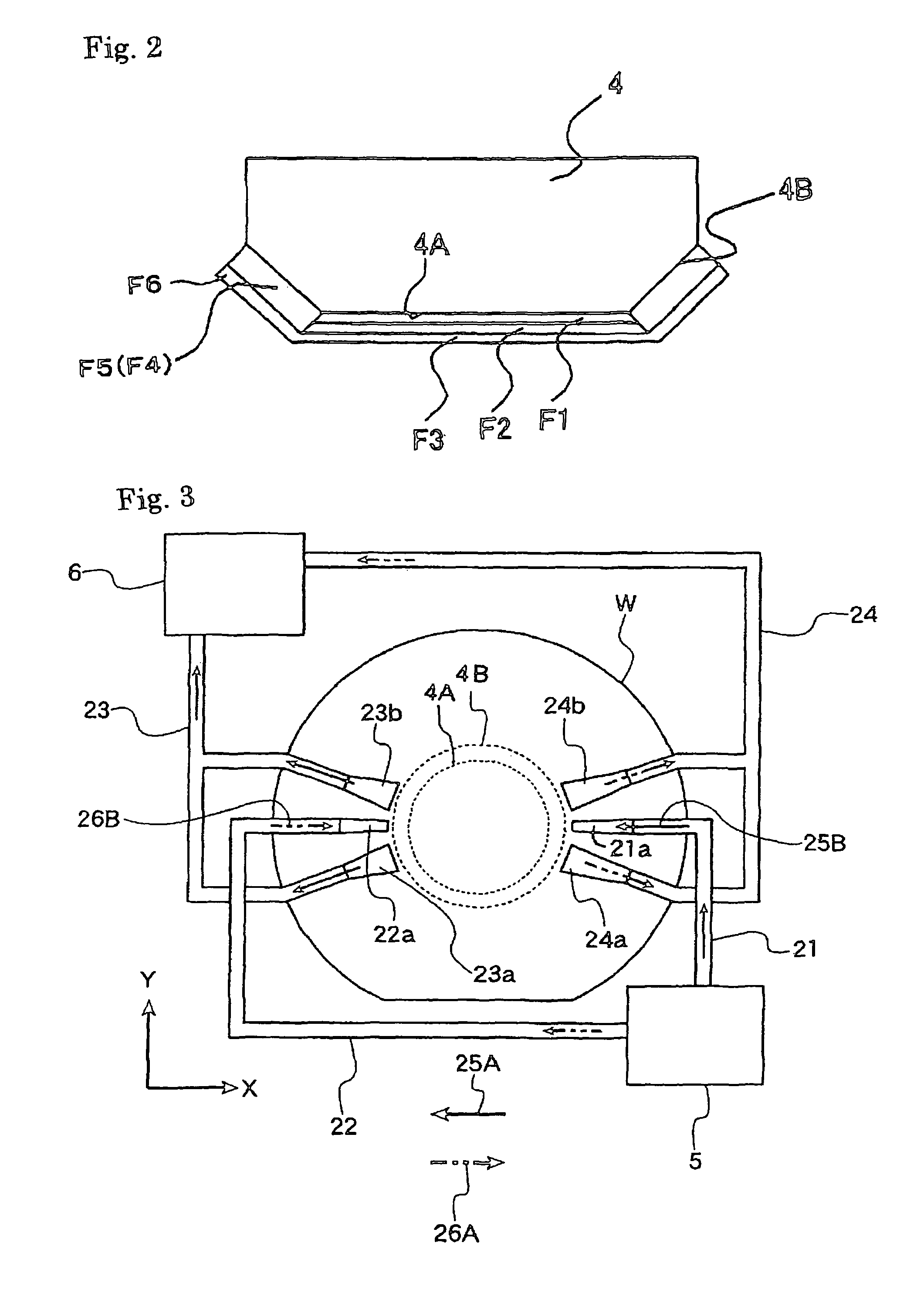
[0182]As shown in FIG. 1, the projection exposure apparatus according to this embodiment is pro...
embodiment 2
[0226]A projection exposure apparatus is configured as similar to that of Embodiment 1 except that a magnesium fluoride (MgF2) film is formed at the tip portion 4A of the optical element 4, or in other words, at the portion contacting the liquid 7, as the single-layered anti-dissolution film by use of the vacuum vapor deposition method.
[0227]According to the projection exposure apparatus of this Embodiment 2, the single-layered anti-dissolution film is formed on the surface of the optical element, and it is thereby possible to prevent dissolution of the optical element. Further, it is possible to reduce the interface as compared to the multilayer film. Therefore, it is possible to minimize an adverse effect attributable to a chemical reaction which is apt to occur when the liquid infiltrates into the interface of the protective layer serving as the anti-dissolution film. Moreover, it is easier to form the film as compared to formation of the anti-dissolution film including the multi...
embodiment 3
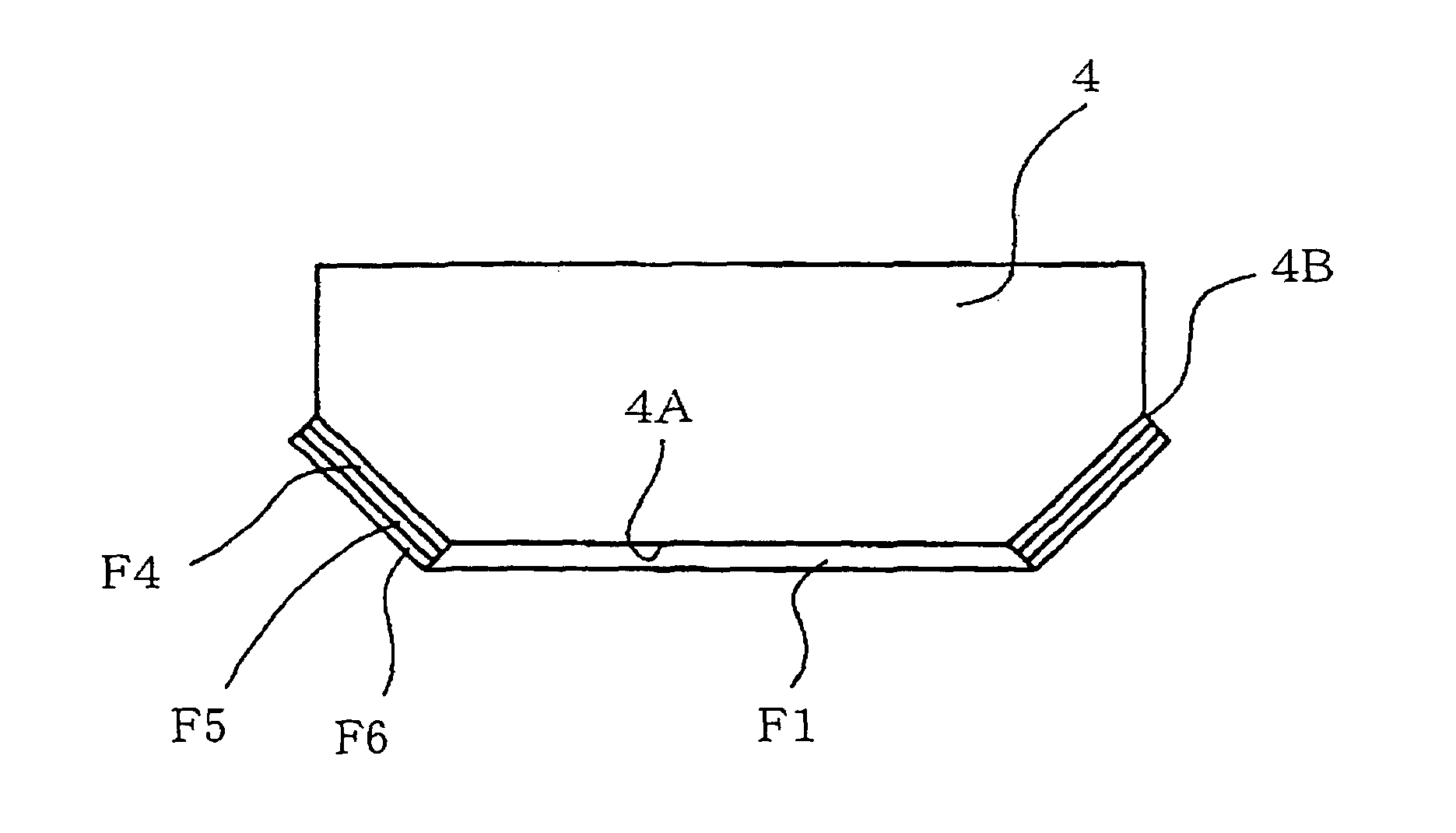
[0229]A projection exposure apparatus is configured as similar to Embodiment 1 except that the transmissive optical element 4 is modified as shown in FIG. 6 and as described below.
[0230](i) The magnesium fluoride (MgF2) film F1 is formed at the tip portion 4A of the optical element 4 on the wafer W side, or in other words, at the portion where the exposure light beam passes through, constituted of the single-layered anti-dissolution film by use of the vacuum vapor deposition method.
(ii) The tantalum (Ta) film serving as the adhesion reinforcing film F4 is formed on the tapered surface 4B of the transmissive optical element 4, or in other words, at the portion where the exposure light beam does not pass through by use of the sputtering method. The adhesion reinforcing film F4 is used for improving adhesion between the tapered surface 4B of the transmissive optical element 4 and the metal anti-dissolution film (the anti-dissolution film) F5 to be described later.
(iii) A metal film mad...
PUM
 Abstract
Description
Claims
Application Information


