Light emitting display device with first and second transistor films and capacitor with large capacitance value

a technology of transistor film and capacitor, which is applied in the direction of instruments, static indicating devices, etc., can solve the problems of high manufacturing cost, large power consumption, uneven display, etc., and achieve the effect of suppressing the effect of characteristic shi

Inactive Publication Date: 2012-04-17
CANON KK
View PDF14 Cites 9 Cited by
  • Summary
  • Abstract
  • Description
  • Claims
  • Application Information

AI Technical Summary

Benefits of technology

[0022]It is an object of the present invention to provide a light emitting display device using a drive circuit comprised of only unipolar thin film transistors, which is capable of suppressing an effect of characteristic shifts of the thin film transistors due to an applied voltage, and is capable of being applied to a large and high-resolution light emitting display device.
[0033]According to the present invention, each pixel has a drive circuit including a current mirror circuit formed of a pair of thin film transistors having the same polarity. The pair of thin film transistors have a common source terminal connected to one end of the light emitting device and connected to the first line through the first switch, and there is provided a capacitor between the gate terminal and the source terminal. With this configuration, it is possible to provide a light emitting display device using a drive circuit comprised of only unipolar thin film transistors, which is capable of suppressing the effect of the characteristic shifts of the thin film transistors due to the applied voltage, and is capable of being applied to a large and high-resolution light emitting display device.

Problems solved by technology

On the other hand, when there is variation in characteristics of the TFT, the current supplied to the organic EL device LED varies, whereby display unevenness appears.
The p-Si TFT can be produced with a high mobility at low working voltage, but manufacturing costs therefor are high.
On the other hand, the a-Si TFT or the OS TFT can be produced at low cost with a small number of manufacturing steps, but requires a high working voltage and large power consumption because the a-Si and OS the TFT have a lower mobility than the p-Si TFT.
For example, a p-type semiconductor having a high mobility has not been obtained with a-Si or a metal oxide, so it is difficult to form a p-type TFT.
In addition, with regard to the OS, the n-type semiconductor and the p-type semiconductor that have a high mobility are made of different materials, which requires twice as many processes and makes it difficult to manufacture the TFT at low costs.
Therefore, in the prior arts particularly in a case of supplying a low current corresponding to low gradation from the outside, a long time is necessary for charging the line load.
In this case, it takes a long time to perform an operation for setting the voltage at the gate terminal of the TFT provided within the drive circuit to be equal to the voltage at which the current from the outside flows, according to the threshold and the mobility of the TFT, which makes it difficult to apply the organic EL device to a display device with high-resolution and a large screen.

Method used


Image

  • Light emitting display device with first and second transistor films and capacitor with large capacitance value
  • Light emitting display device with first and second transistor films and capacitor with large capacitance value
  • Light emitting display device with first and second transistor films and capacitor with large capacitance value

Examples


example 1

[0082]First, Example 1 of the present invention will be described.

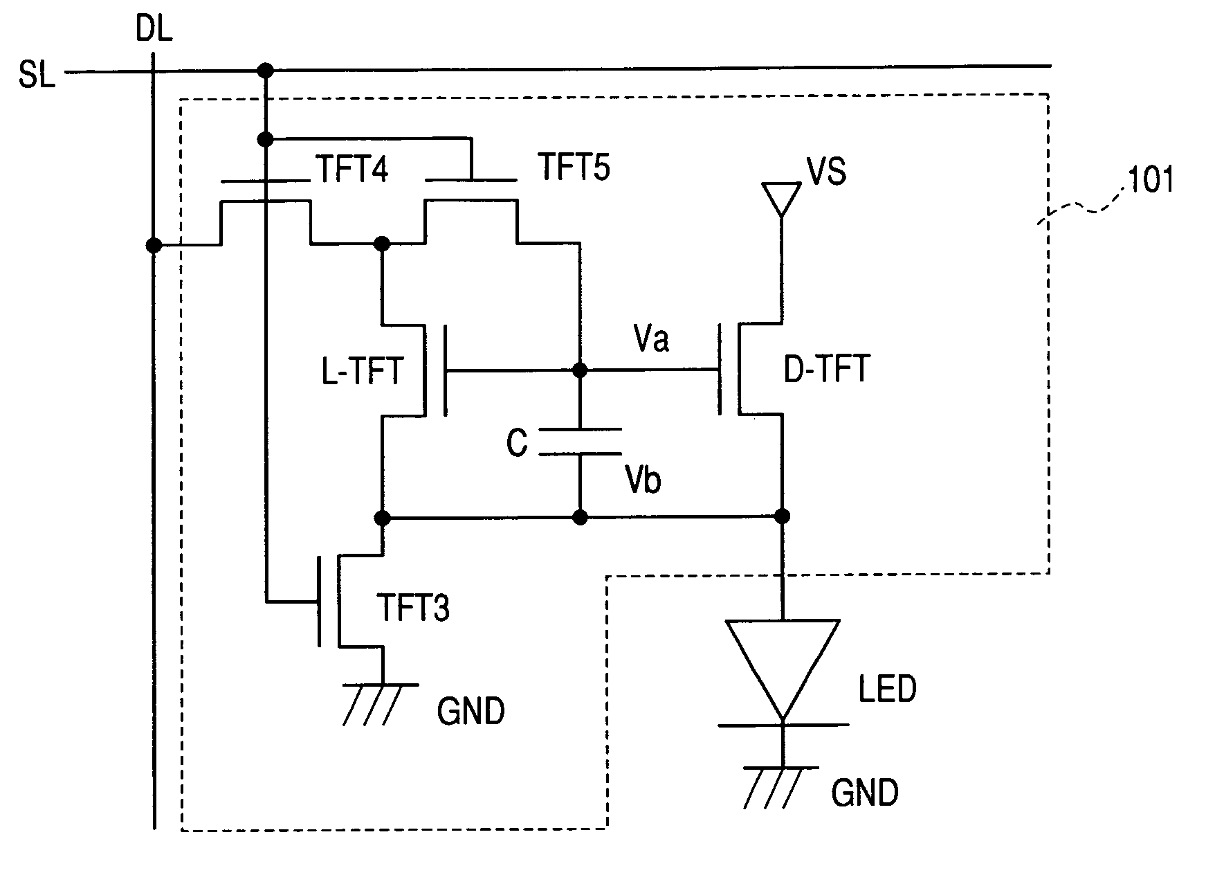
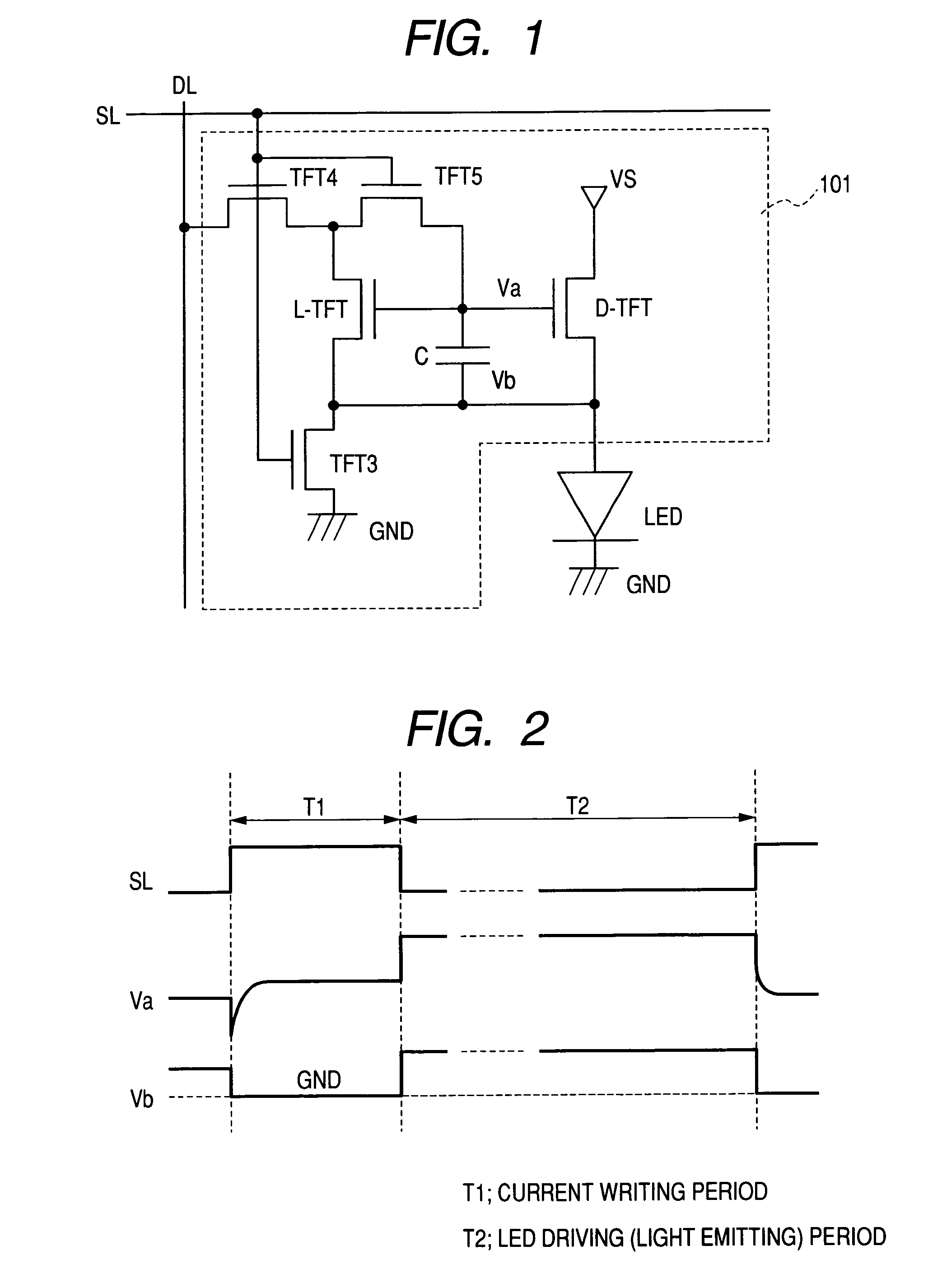
[0083]A configuration of this example is illustrated in FIG. 1. The light emitting display device illustrated in FIG. 1 is an organic EL display device (AM-type organic EL display) including pixels each having an organic EL device LED having a cathode terminal connected (grounded) to a ground line GND, and a drive circuit 101 for driving the organic EL device LED.

[0084]The organic EL device LED has an anode electrode, an organic material light emitting layer and a cathode electrode, which are laminated in the stated order from the bottom.

[0085]The drive circuit 101 includes a first n-type TFT (hereinafter, referred to as “L-TFT”), a second n-type TFT (hereinafter, referred to as “D-TFT”), a third n-type TFT (hereinafter, referred to as “TFT3”), a fourth n-type TFT (hereinafter, referred to as “TFT4”), a fifth n-type TFT (hereinafter, referred to as “TFT5”), and a capacitor C. The L-TFT and the D-TFT are each formed of...

example 2

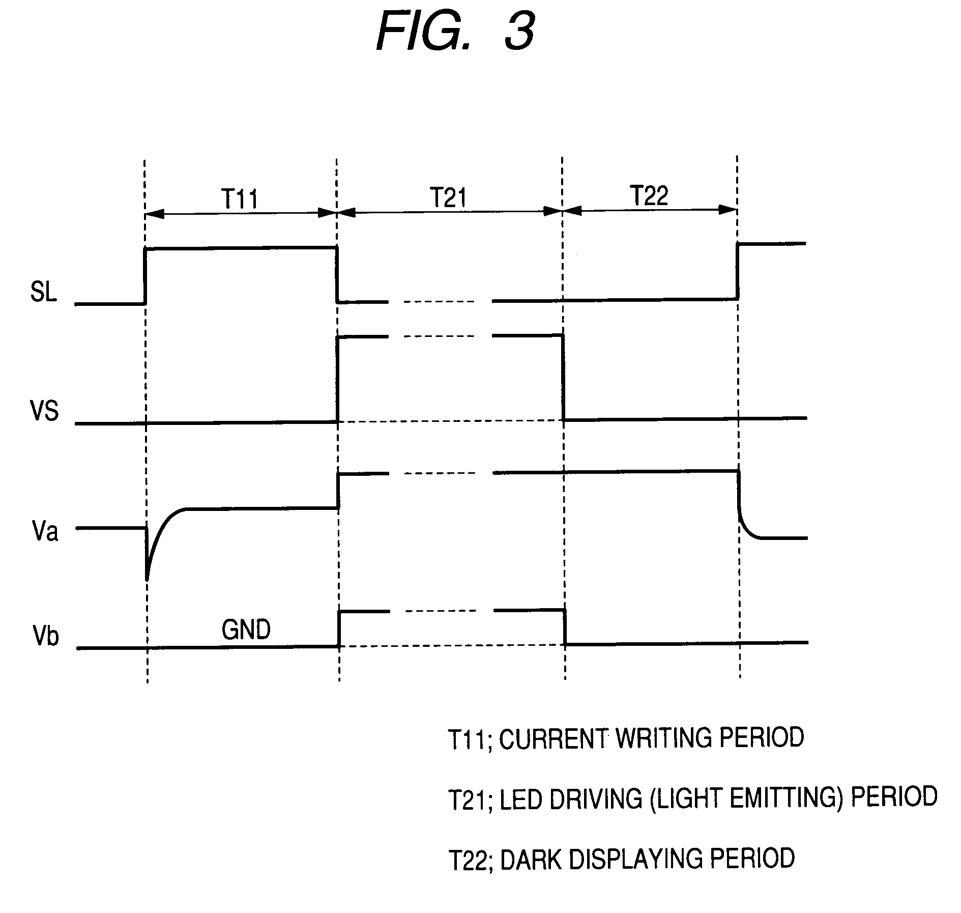
[0106]Next, Example 2 of the present invention will be described. A configuration of a light emitting display device according to this example is identical with that of Example 1. Note that this example is characterized in that the voltage of the power supply line VS is varied.

[0107]Hereinafter, referring to a timing chart illustrated in FIG. 3, operations according to this example will be described.

[0108]First, in a period T11 in which the signal of the scan line SL is set to the H level, and the voltage of the power supply line VS is set to be at the same potential as the voltage of the ground line GND (hereinafter, referred to as “GND”) (current writing period), the TFT3, the TFT4, and the TFT5 are turned on. During the period T11, when the TFT3 is turned on, the voltage of the source terminals of the L-TFT and the D-TFT and the voltage Vb of the anode terminal of the organic EL device LED are at the same potential as that of the voltage of the ground line GND through the TFT3. O...

example 3

[0113]Next, Example 3 of the present invention will be described.

[0114]A configuration of this example is illustrated in FIG. 4. A light emitting display device illustrated in FIG. 4 is an organic EL display device (AM-type organic display) including pixels each having an organic EL device LED having a cathode terminal connected (grounded) to a ground line GND, and a drive circuit 101 for driving the organic EL device LED.

[0115]In the organic EL device LED, an anode electrode, an organic material light emitting layer, and a cathode electrode are laminated in the stated order from the bottom.

[0116]The drive circuit 101 includes a first n-type TFT (hereinafter, referred to as “L-TFT”), a second n-type TFT (hereinafter, referred to as “D-TFT”), a third n-type TFT (hereinafter, referred to as “TFT3”), a fourth n-type TFT (hereinafter, referred to as “TFT4”), and a fifth n-type TFT (hereinafter, referred to as “TFT5”). In addition, the drive circuit 101 includes a sixth n-type TFT (which...


PUM


Abstract

A light emitting display device using a drive circuit formed of only unipolar thin film transistors, which suppresses effects of characteristic shifts of transistors, and is applicable to large, high-resolution light emitting displays. The device includes a pixel having an organic EL device (LED) and a drive circuit thereof. In a current writing period, the drive circuit sets TFT3, TFT4 and TFT5 ON and sets a ground line and one end of LED to the same voltage through TFT3. A current from a data line is supplied to transistors L-TFT and D-TFT forming a current mirror circuit through TFT4 and TFT5, and a voltage between gate and source terminals of L-TFT and D-TFT is retained in a capacitor. During a LED driving period, TFT3, TFT4 and TFT5 are interrupted, and a current flowing between the source and drain of D-TFT is supplied to LED according to the retaining voltage.

Description

TECHNICAL FIELD[0001]The present invention relates to a current load device which achieves a function thereof according to a current to be supplied, and more particularly, to a light emitting display device using a light emitting device as a current load. In particular, the present invention relates to a light emitting display device including a plurality of pixels formed in a matrix form, each of which is comprised of an organic electro-luminescence (hereinafter, referred to as “EL”) device serving as a light emitting device, and a drive circuit for supplying a current to the organic EL device.BACKGROUND ART[0002]An organic EL device is a light emitting device which emits light when a current passes therethrough as in a light emitting diode (LED), and is also called an organic LED (OLED). For the light emitting display device including a plurality of pixels formed in a matrix form, each of which is comprised of the organic EL device and the drive circuit for driving the organic EL ...

Claims


Application Information

Patent Timeline
Patent Type & Authority Patents(United States)
IPC IPC(8): G09G3/30
CPCG09G3/2011G09G3/3241G09G2300/0417G09G2300/0842G09G2300/0861G09G2300/0866G09G2310/0251G09G2310/061G09G2320/0223G09G2320/0233G09G2320/0238G09G2330/025H10K50/85
Inventor ABE, KATSUMI
Owner CANON KK
Why Eureka
Try Eureka