Direct write and additive manufacturing processes

a technology of additive manufacturing and write process, which is applied in the field of direct write process and additive manufacturing process, can solve the problems of difficulty in determining the state of the ink being cured or when the curing has been completed, and achieve the effect of reducing the resistance of the ink and the rate of curing

Active Publication Date: 2012-05-15
BAE SYSTEMS PLC
View PDF16 Cites 10 Cited by
  • Summary
  • Abstract
  • Description
  • Claims
  • Application Information

AI Technical Summary

Benefits of technology

[0015]The present invention overcomes the need in a Direct Write process of placing a substrate in an oven, by instead thermally curing the Direct Write ink in situ. The curing may be performed in an exemplary embodiment using an induction coil through which an oscillating current is passed. The coil is placed above the region to be cured. The oscillating current induces charge movement (eddy currents) in the region to be cured and the resistance to this charge movement causes Joule heating in the affected area and thus curing and sintering the inks. The current required for curing will depend on the dimensions of the area to be cured and its electrical and thermal properties, and will thus vary depending on the specifics of the application. A problem with other curing methods that may use localized radiation (such as laser or lamp radiation) is that it is difficult to ascertain when curing has been completed or indeed what the state of the inks being cured is. An additional advantage of this invention, at least in an exemplary embodiment, is that there may be a degree of self control and inherent process monitoring; as the curing progresses the resistance of the inks decreases and thus the rate of curing may decrease. This effect may be monitored and curing automatically adjusted as the curing progresses.

Problems solved by technology

A problem with other curing methods that may use localized radiation (such as laser or lamp radiation) is that it is difficult to ascertain when curing has been completed or indeed what the state of the inks being cured is.

Method used


Image

  • Direct write and additive manufacturing processes
  • Direct write and additive manufacturing processes
  • Direct write and additive manufacturing processes

Examples


example

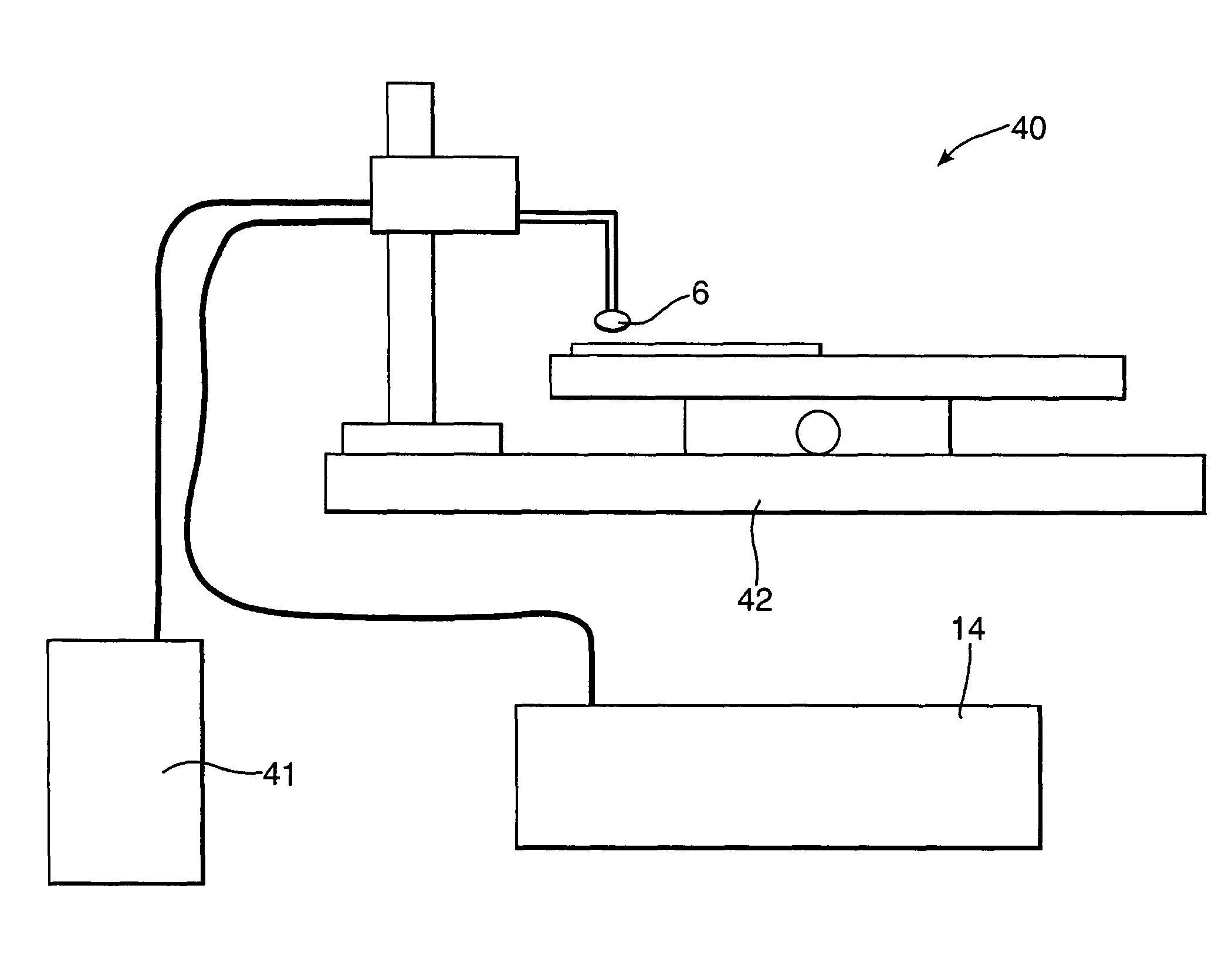
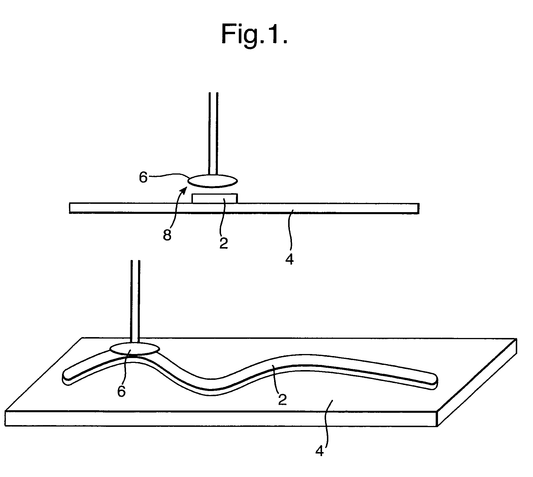
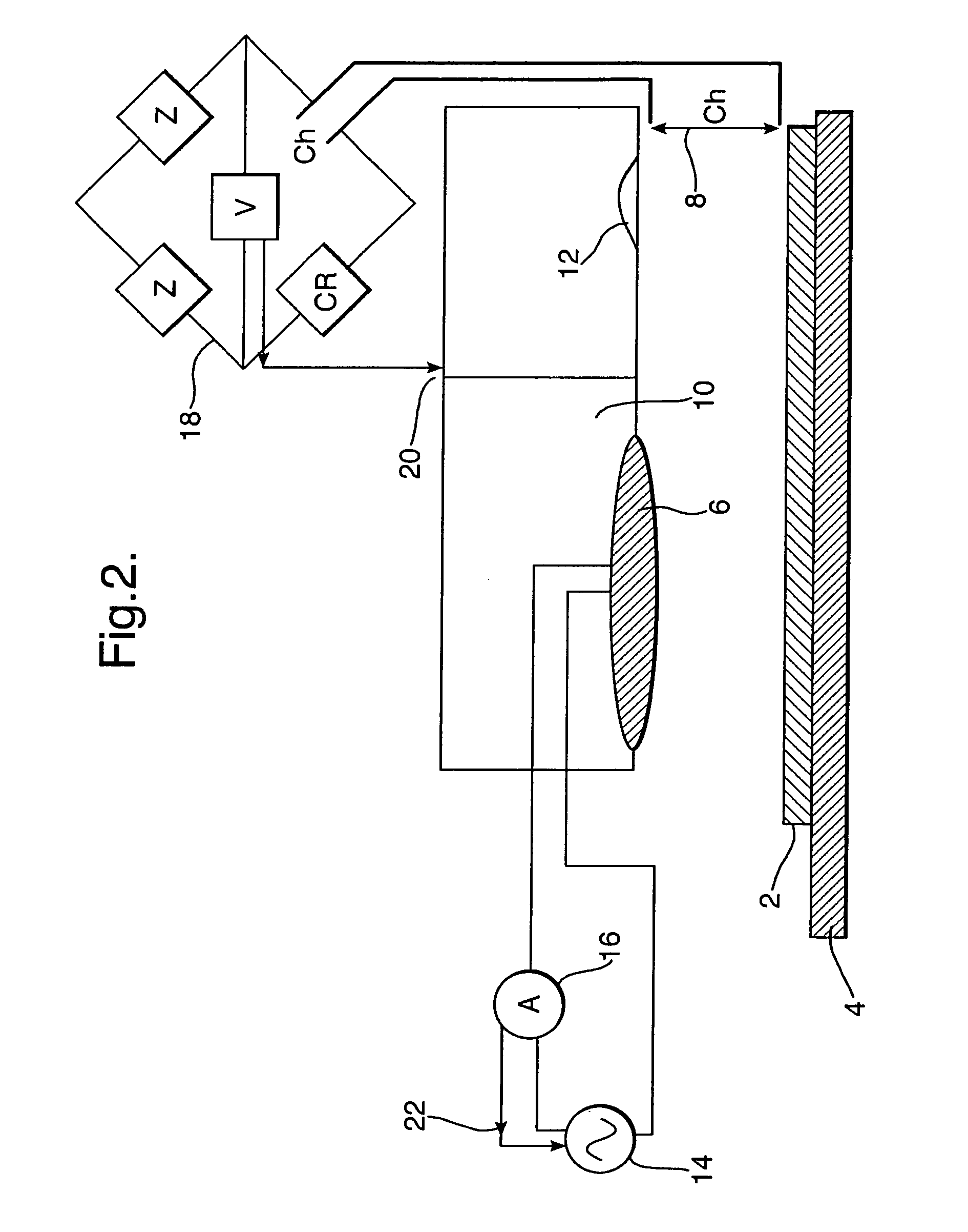
[0046]An nScrypt “Smart Pump” is specified to dispense lines down to 50 μm wide and onto conformal surfaces where the angle of the substrate is below 30°. The theoretical track resolution with a “micro pen” system is 100 μm using a 75 μm outer diameter tip, although the narrowest lines produced to date are approximately 230 μm wide using a 175 μm outer diameter tip.

[0047]To assist with the materials characterization and process optimization, an Intertronics DK118 Digital Dispenser is used, which is a bench top syringe system using a simple pressure regulator to provide material flow. The output pressure can be set from IPsi to 100 Psi in increments of 1 Psi and the barrel suck-back feature prevents low viscosity materials from dripping. An I / O port allows the dispenser to be interfaced with external devices. The resolution of this dispensing technique is limited by the size and tolerance of the nozzles available. The nozzles have a stainless steel barrel and it is the outer diameter...


PUM

PropertyMeasurementUnit
widthaaaaaaaaaa
widthaaaaaaaaaa
widthaaaaaaaaaa

Abstract

A Direct Write method of forming components on a substrate by deposition of ink by thermally curing the ink in situ, which method overcomes the need for curing by placing the substrate in an oven. The curing is performed in an exemplary embodiment using an induction coil (6) through which an oscillating current is passed. The coil (6) is placed above the region in which Direct Write ink has been deposited. The oscillating current induces eddy currents in the ink to cause heating of the ink and thus fix the ink by curing, sintering etc.

Description

RELATED APPLICATION INFORMATION[0001]This application is a United States National Phase Patent Application of International Patent Application No. PCT / GB2008 / 050390 which was filed on May 30, 2008, and claims priority to British Patent Application No. 0710415.1, filed on Jun. 1, 2007, and claims priority to European Patent Application No. 07270028.9, filed on Jun. 1, 2007, the disclosures of each of which are incorporated herein by reference.FIELD OF THE INVENTION[0002]The present invention concerns improvements relating to Direct Write processes and additive manufacturing processes.BACKGROUND INFORMATION[0003]The term Direct Write is commonly used to describe a range of technologies which allows the fabrication of two or three-dimensional functional structures using processes that are compatible with being carried out directly onto potentially large complex shapes (DTI Report February 2004 “Direct Writing”). Direct Write manufacturing techniques include: Ink jet, Micro-spray, Quill...

Claims


Application Information

Patent Timeline
Patent Type & Authority Patents(United States)
IPC IPC(8): B41J2/01
CPCB29C67/0055H05K3/12H05K1/095H05K3/1241H05K2203/101H05K2203/1105B29C64/106B33Y30/00B33Y10/00B33Y80/00
Inventor SIDHU, JAGJITMCDONALD, JENNIFER LAURA
Owner BAE SYSTEMS PLC
Why Eureka
Try Eureka