High performance InAs-based devices
- Summary
- Abstract
- Description
- Claims
- Application Information
AI Technical Summary
Benefits of technology
Problems solved by technology
Method used
Image

Examples
Embodiment Construction
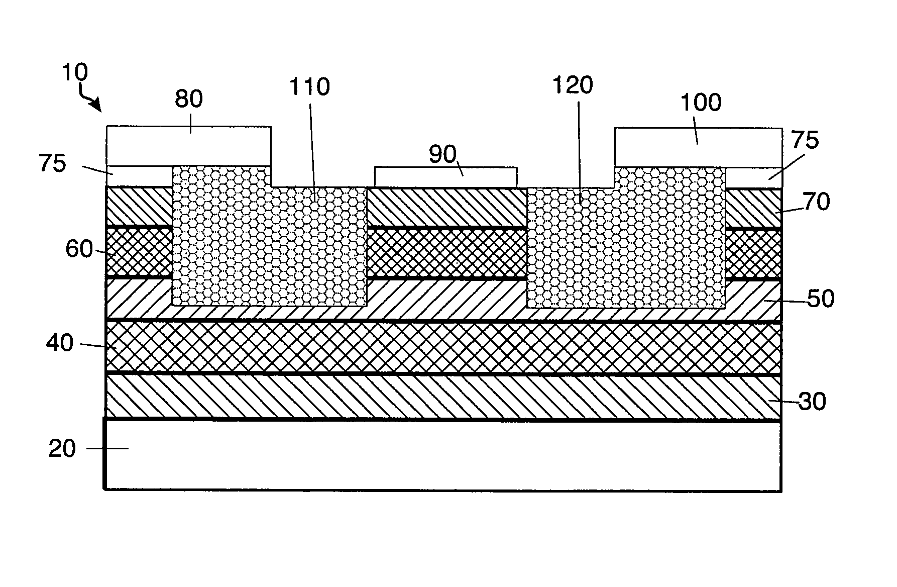
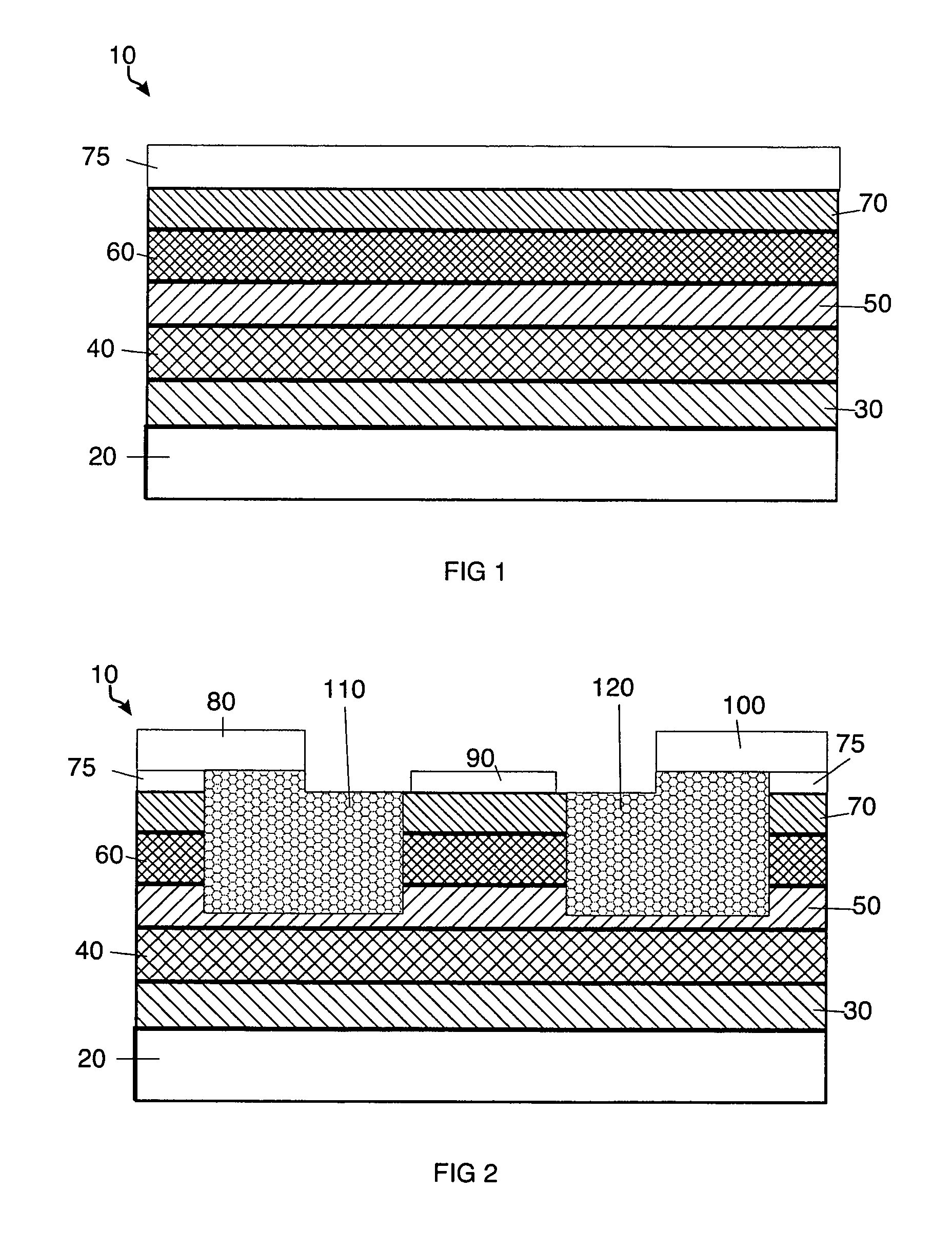
[0020]In one exemplary embodiment, to provide FET devices such as, for example, HEMT with high mobility and good electron and hole confinement, a material layer structure 10 may be grown as shown in FIG. 1. To obtain high mobility, a high conduction band barrier and to enable higher performance, the quantum well layer 60 is confined by using wider band-gap InAsP layers 50 and 70 as the barriers in the material layer structure 10. The InAsP material may, for example, have the following properties: InAs0.5P0.05 or InAs0.6P0.4. The quantum well layer 60 may be composed of, for example, InAs material about 100 Å in thickness. The wider band-gap layers 50 and 70 may be composed of, for example InAsP material from about 200 Å to about 600 Å. Layer 75 is a contact layer and may be composed of InAs or an alloy containing at least 75% InAs, with a thickness of about 100 Å to 500 Å.
[0021]The quantum well layer 60 confined by the wider band-gap layers 50 and 70 of the material layer structure ...
PUM
 Abstract
Description
Claims
Application Information
 - R&D Engineer
- R&D Manager
- IP Professional
- Industry Leading Data Capabilities
- Powerful AI technology
- Patent DNA Extraction
Browse by: Latest US Patents, China's latest patents, Technical Efficacy Thesaurus, Application Domain, Technology Topic.
© 2024 PatSnap. All rights reserved.Legal|Privacy policy|Modern Slavery Act Transparency Statement|Sitemap