IC chip mounting package provided with IC chip located in device hole formed within a package base member

a technology for mounting packages and ic chips, which is applied in the direction of optics, instruments, printed circuit aspects, etc., can solve the problems of reducing the reliability of sealing at the connected section using sealing resin, the sealing resin may not be sufficiently permeated between the ic chip and the circuit board, and the sealing resin may not be easy to crack, so as to avoid insufficient resin filling and improve the filling performance

Active Publication Date: 2012-06-05
SHENZHEN TOREY MICROELECTRONIC TECH CO LTD
View PDF9 Cites 2 Cited by
  • Summary
  • Abstract
  • Description
  • Claims
  • Application Information

AI Technical Summary

Benefits of technology

[0015]Namely, in a conventional SOF structure which directly connects the IC chip to the circuit board, the IC chip and the circuit board can be sealed without any air bubbles or the like generating, by potting the sealing resin so as to draw around the IC chip, which causes the sealing resin to permeate between the IC chip and the circuit board by capillary action.
[0031]According to the structure, resin filling performance is improved, particularly in a space between the IC chip and the interposer. This makes it possible to avoid insufficient resin filling.

Problems solved by technology

However, in the structure in which the IC chip 104 and the circuit board 107 are connected via the interposer 101 as disclosed in Patent Literature 1, problems occur such as a decrease in sealing reliability at a connected section using sealing resin, which decrease is caused by opening the device hole 107A in the circuit board 107.
As a result, the sealing resin may not be sufficiently permeated between the IC chip and the circuit board.
Therefore, it is difficult for the sealing resin to crack due to the thermal expansion or contraction of the sealing resin.

Method used


Image

  • IC chip mounting package provided with IC chip located in device hole formed within a package base member
  • IC chip mounting package provided with IC chip located in device hole formed within a package base member
  • IC chip mounting package provided with IC chip located in device hole formed within a package base member

Examples


Embodiment Construction

[0044]One embodiment of the present invention is described below with reference to FIGS. 1 through 11. The following description includes various limitations. These are technically preferred in the implementation of the present invention, but by no means limiting the scope of the present invention.

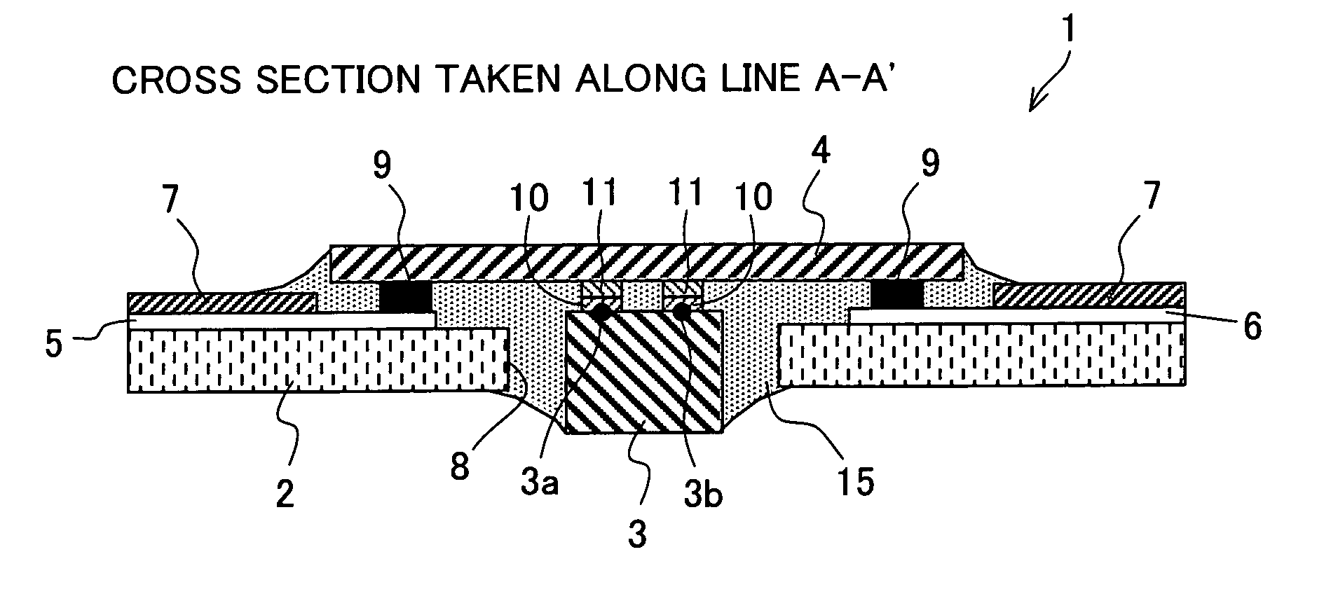
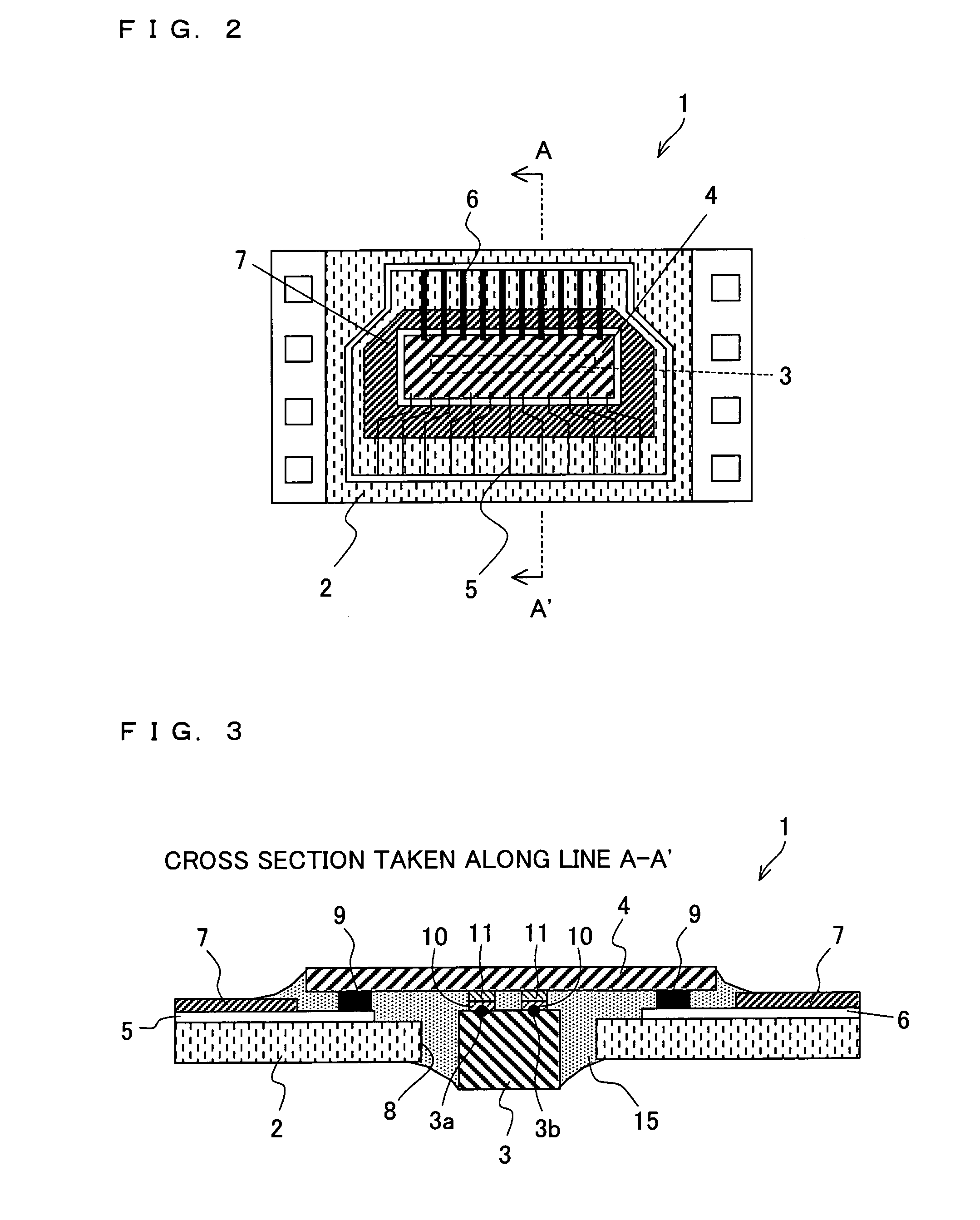
[0045]FIG. 2 is a plan view illustrating a structure of an IC chip mounting package 1 in accordance with the present embodiment. FIG. 3 is a cross sectional view of the IC chip mounting package 1 taken along line A-A of FIG. 2.

[0046]The mounting package 1 briefly is arranged including a film base member (tape carrier) 2, which is a package base member, an IC chip 3, and an interposer 4. FIG. 2 illustrates the mounting package 1 from a side on which the interposer 4 is provided. For convenience in explanation, FIG. 3 is illustrated so as to have the IC chip 3 face downwards in the figure. FIG. 3 illustrates one part of a cross section taken along line A-A′.

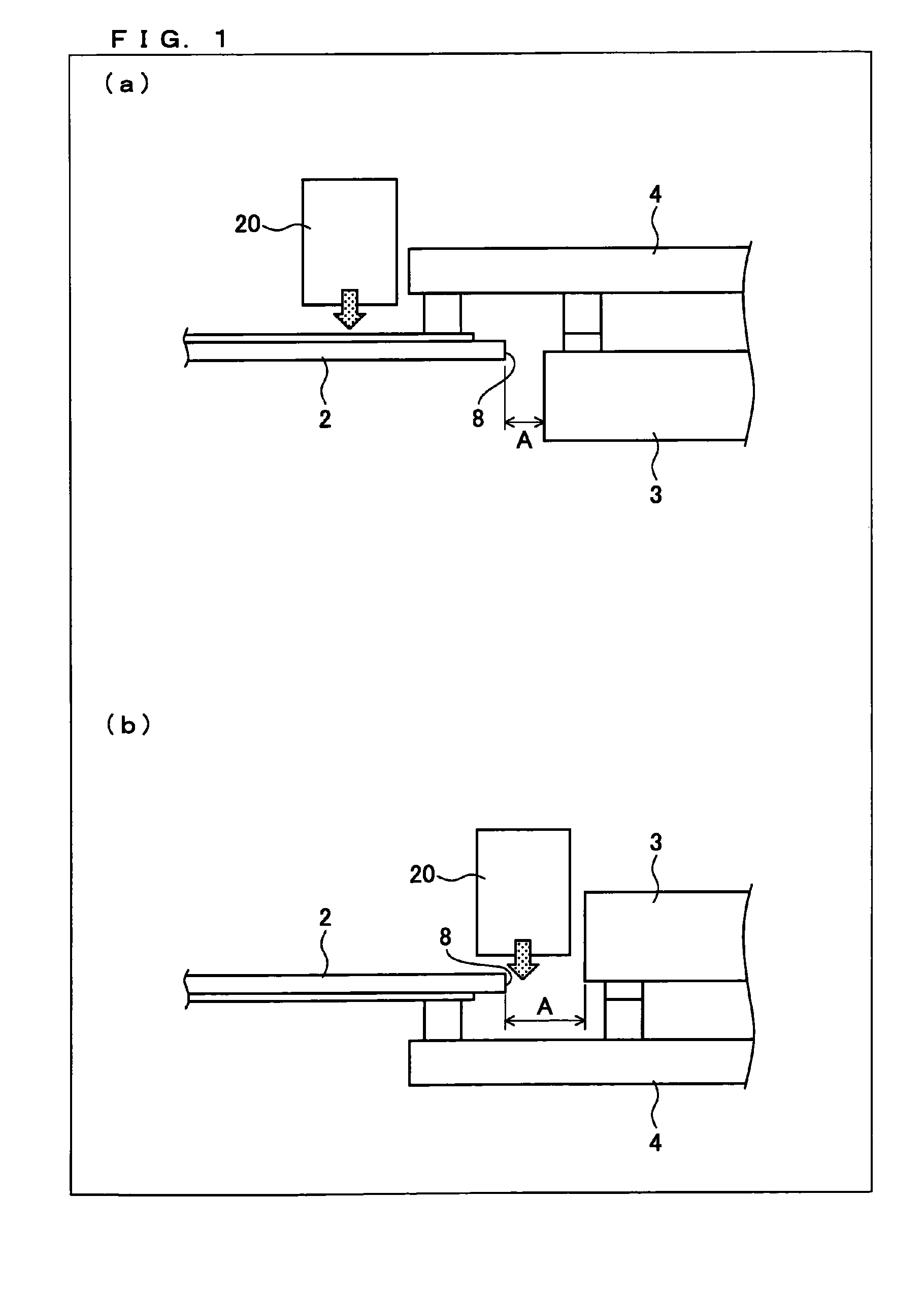
[0047]In the mounting package 1, t...


PUM


Abstract

In one embodiment of the present invention, an IC chip mounting package is arranged such that an IC chip and a film base member are connected via an interposer, and a section in which the IC chip, the film base member, and the interposer are connected is sealed with sealing resin. The sealing resin is provided by potting sealing resin around the interposer via a potting nozzle, or is provided by potting the sealing resin around the IC chip, that is, via a device hole. Moreover, the sealing resin has a coefficient of linear expansion of not more than 80 ppm / ° C., a viscosity of not less than 0.05 Pa·s but not more than 0.25 Pa·s, and also includes filler having a particle size of not more than 1 μm.

Description

TECHNICAL FIELD[0001]The present invention relates to a package for mounting an IC chip which includes, for example, finely pitched terminals.BACKGROUND ART[0002]With the development of a liquid crystal display apparatus with high definition and high performance, a liquid crystal, driver (IC chip) incorporated in the liquid crystal display apparatus is required to have an increased number of outputs, and also a reduced chip size.[0003]In order to accomplish the increased number of outputs in an IC chip reduced in chip size, it is required for the chip to have bumps made in a fine pitch (smaller pitch). Recently, an SOF (System On Film), also referred to as COF (Chip On Film)) is often used. The SOF can realize the fine pitch and includes a bare chip liquid crystal driver.[0004]In the latest SOF package, inner leads on a tape carrier are bonded to bumps on an IC chip by the application of heat and pressure so that the tape carrier is brought into conduction with the IC chip. However,...

Claims


Application Information

Patent Timeline
Patent Type & Authority Patents(United States)
IPC IPC(8): H01L23/18H01L21/56H01L23/48
CPCH01L21/563H01L23/13H01L23/3121H01L23/49833H05K1/182G02F1/1345H01L2224/92125H01L2224/73204H01L2224/32225H01L2224/16225H05K2201/10977H05K2201/10727H05K3/284H05K1/189H01L23/4985H01L2224/73203H01L2924/00
Inventor KUDOSE, SATORUNAKAGAWA, TOMOKATSUKATOH, TATSUYA
Owner SHENZHEN TOREY MICROELECTRONIC TECH CO LTD
Why Eureka
Try Eureka