Wafer polishing device and method

a polishing device and polishing technology, applied in the direction of edge grinding machines, manufacturing tools, lapping machines, etc., can solve the problems of difficult, but likely not to achieve the lowering of pressure per unit area, and achieve the improvement of load application control accuracy for polishing processing, reducing the difficulty of polishing, and improving the accuracy of polishing processing.

Inactive Publication Date: 2012-07-03
SONY CORP
View PDF15 Cites 20 Cited by
  • Summary
  • Abstract
  • Description
  • Claims
  • Application Information

AI Technical Summary

Benefits of technology

[0008]If the polishing processing is performed on the bevel portion of the wafer using the abrasive film, to perform the polishing processing at a low load, it is conceivable to increase the contact area between the abrasive film and the bevel portion to thereby lower pressure per unit area.
[0010]To perform the polishing processing at a low load, it is conceivable that the pressurizing force of the abrasive film to the bevel portion of the wafer is reduced to lower pressure per unit area. More specifically, it is conceivable that without load application from the rear side of the abrasive film, polishing pressure is controlled by the tension of the abrasive film to reduce the pressurizing force of the abrasive film to the bevel portion of the wafer to thereby lower pressure per unit area.
[0013]It is desirable, therefore, to provide a wafer polishing device and method that can perform, even to perform polishing processing on the outer circumferential end-edge of a wafer which is a workpiece to be polished using a belt-like abrasive member represented by an abrasive film, the polishing processing at a low load, and that can improve the accuracy of load application control during the polishing processing, thereby achieving the higher-accuracy and higher-efficiency of the polishing processing.
[0015]In the wafer polishing device configured as above, the belt-like abrasive member having the non-abrasive sections disposed on both the sides of the abrasive grain section is brought into contact with the outer circumferential end-edge of the wafer. Specifically, since the non-abrasive sections as well as the abrasive grain section are brought into contact with the outer circumferential end-edge of the wafer, the contact area of the abrasive member with the outer circumferential end-edge of the wafer is increased according to the non-abrasive sections. In addition, when the abrasive member is brought into contact with the outer circumferential end-edge of the wafer, the two guide surfaces of the guide member press the respective rear surfaces of the non-abrasive sections of the abrasive member. Thus, the abrasive member is brought into contact with the outer circumferential end-edge while conforming to the shape of the outer circumferential end-edge of the wafer. In addition, since the abrasive grain section is not directly be pressed to the circumferential end-edge from the rear side thereof, the pressurizing force of the abrasive grain section does not become excessive.
[0016]According to the embodiment of the present invention, the increased contact area of the belt-like abrasive member with the outer circumferential end-edge of the wafer can lower pressure per unit area. The abrasive member conforming to the outer circumferential end-edge of the wafer can achieve the uniform pressurization of the abrasive member to the outer circumferential end-edge. Further, the pressurizing force of the abrasive grain section does not become excessive. Thus, even if the polishing processing is performed on the outer circumferential end-edge of the wafer which is a workpiece to be polished by use of the belt-like abrasive member, it can be done at a low load and the accuracy of load application control for the polishing processing can be improved. As a result, the higher-accuracy and efficiency of the polishing processing can be achieved.

Problems solved by technology

It is difficult, however, for the method performed using the traditional abrasive film to perform the polishing processing at a low load for the reason described below.
Consequently, it is likely not to achieve lowering of pressure per unit area.

Method used


Image

  • Wafer polishing device and method
  • Wafer polishing device and method
  • Wafer polishing device and method

Examples


first embodiment

[0029]A description will first be given of a first embodiment of the present invention.

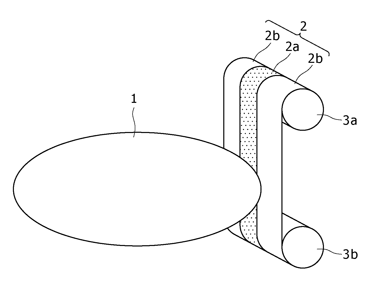
[0030]FIGS. 1 to 3 are explanatory views illustrating a schematic configurational example of a wafer polishing device according to the first embodiment.

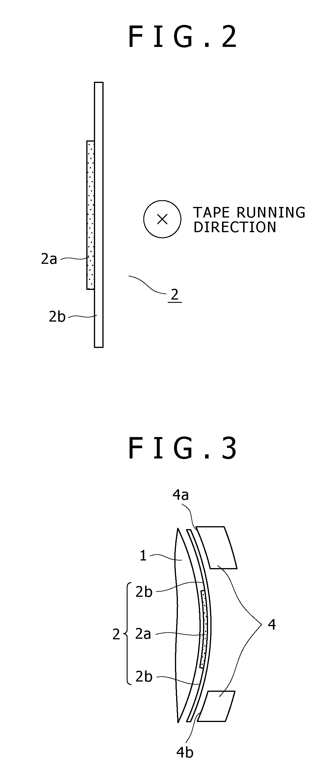
[0031]Referring to FIG. 1, the wafer polishing device of the first embodiment is configured such that an abrasive tape 2 which is a belt-like polishing member is run in a direction crossing a bevel portion while being brought into contact with an outer circumferential end-edge (the bevel portion) of a wafer 1 which is a workpiece to be polished. More specifically, a feed roll 3a and a recovery roll 3b for the abrasive tape 2 are respectively arranged above and below the wafer 1. The abrasive tape 2 is moved upward or downward between the rolls 3a, 3b, i.e., in a direction vertical to the circumferential direction of the wafer 1. These rolls 3a, 3b achieve a function as a polishing member driving device by way of one specific example.

[0032]Referring...

second embodiment

[0051]A description is next given of a second embodiment of the present invention.

[0052]FIG. 4 is an explanatory view illustrating a schematic configurational example of a wafer polishing device according to the second embodiment. An abrasive tape 5 of the wafer polishing device in the figure is different from that of the first embodiment described above.

[0053]Similarly to the first embodiment, the abrasive tape 5 has an abrasive grain section 5a and non-abrasive sections 5b. The non-abrasive sections 5b are located on both sides of the abrasive grain section 5a. In addition, the abrasive grain section 5a and the non-abrasive sections 5b are formed as a single piece.

[0054]However, unlike the first embodiment, the abrasive tape 5 is such that the non-abrasive section 5b is formed of a base material made of a soft material such as nonwoven cloth and abrasive grains are impregnated into the base material to form the abrasive grain section 5a.

[0055]If the abrasive tape 5 formed as abov...

third embodiment

[0056]A description is next given of a third embodiment of the present invention.

[0057]FIG. 5 is an explanatory view illustrating a schematic configurational example of a wafer polishing device according to the third embodiment.

[0058]In the configurational example of the first embodiment described above, the excessive pressurizing force of the abrasive grain section 2a is avoided without directly applying pressure to the abrasive grain section 2a from the rear side thereof. However, in the configurational example described here, a pressurizing plate 6a is disposed on the rear side of the abrasive grain section 2a and a pressure control mechanism 6b for the pressurizing plate 6a is provided on the rear side of the pressurizing plate 6a. This is different from the first or second embodiment.

[0059]The pressurizing plate 6a is not particularly restricted as long as it is a plate-like member capable of applying pressure to the abrasive grain section 2a. Also the pressure control mechanis...


PUM

PropertyMeasurementUnit
thicknessaaaaaaaaaa
shapeaaaaaaaaaa
pressureaaaaaaaaaa

Abstract

Disclosed herein is a wafer polishing device including: an abrasive member driving device adapted to run a belt-like abrasive member in a direction crossing an outer circumferential end-edge of a wafer which is a wafer to be polished while bringing a belt-like abrasive member into contact with outer circumferential end-edge of the wafer, the abrasive member having non-abrasive sections disposed on both sides of an abrasive grain section; and a guide member having two guide surfaces shaped to conform to the outer circumferential end-edge of the wafer, the two guide surface being adapted to press, from rear sides of the non-abrasive sections, the respective non-abrasive sections of the abrasive member run by the abrasive member driving device.

Description

BACKGROUND OF THE INVENTION[0001]1. Field of the Invention[0002]The present invention relates to a wafer polishing device and method for polishing the outer circumferential end-edge of a wafer.[0003]2. Description of the Related Art[0004]In the semiconductor device manufacturing step, a front-surface condition of an outer circumferential end-edge portion (a chamfered portion of an end) called a bevel portion attracts attention in view of an improvement in yield. This is because unnecessary materials, damage, etc. left on the bevel portion fall away and adhere to the device front surface during undergoing various steps, which exerts a harmful influence on product yields.[0005]Because of this, it have been proposed in recent years that polishing processing is performed on the bevel portion of a wafer as a sub-step of a semiconductor device manufacturing step to suppress the occurrence of foreign matter from the bevel portion. See e.g. Japanese Patent Laid-open No. 2001-345294.[0006]As...

Claims


Application Information

Patent Timeline
Patent Type & Authority Patents(United States)
IPC IPC(8): B24B1/00
CPCB24B9/065B24B21/02B24B37/042
Inventor SAKAIRI, TAKASHI
Owner SONY CORP
Why Eureka
Try Eureka