Field effect transistor source or drain with a multi-facet surface

a field effect transistor and surface technology, applied in the field of field effect transistors, can solve the problems of unfavorable scaled devices, unfavorable approach, and affecting the drive current, so as to improve the control of electrostatics, precise control of surface chemistry, and enhance current flow

Active Publication Date: 2012-07-03
ACORN SEMI LLC
View PDF3 Cites 29 Cited by
  • Summary
  • Abstract
  • Description
  • Claims
  • Application Information

AI Technical Summary

Benefits of technology

[0012]In various embodiments, the present invention provides a FET having a metal S / D and a semiconductor channel, wherein a surface of the semiconductor channel region (i.e., the region in which a conductive charge layer may be formed under the gate) proximate to the metal S / D is formed of two or more equivalent lattice planes (e.g., {111} surfaces), the planes meeting at an angle with respect to one another such that a surface of the metal S / D proximate to the semiconductor channel forms an angled feature. The equivalent lattice planes may form a convex feature, meaning that the surface of the metal S / D proximate to the semiconductor channel will form a concave feature, or the equivalent lattice planes may form a concave feature, meaning that the surface of the metal S / D proximate to the semiconductor channel will form a convex feature. Such a convex metal S / D shape may enhance current flow between the S / D and the channel relative to that which would occur in the absence of the angled feature. Alternatively, for short channels a concave metal S / D shape provides a better control of the electrostatics than would be experienced in the absence of the angled feature.
[0013]The semiconductor channel proximate the metal S / D may be primarily a single crystal semiconductor, for example silicon (Si). Thus, the well-defined crystallographic surfaces, i.e., the equivalent lattice planes, may be formed, in part, using an etch with a KOH solution, a TMAH solution, a NH4OH solution, or similar etchant. The metal that makes up the S / D may then be deposited on the well-defined crystallographic surfaces, which form facets in the semiconductor channel. In some cases, a thin passivation layer may be advantageously introduced (e.g., by way of epitaxial growth) between the metal S / D and the semiconductor channel. The atomically flat facets exposed by the etch may advantageously enable the formation of a uniform and controllable passivation layer by allowing for a more precise control of the surface chemistry as compared to a rough surface. In some cases, the channel direction and the S / D interface are selected so that the TMAH or KOH wet etch process substantially stops on the desired {111} facets, i.e., the {111} family of equivalent lattice planes, enabling a precise positioning of the interface. This control derives from the fact that these wet etch processes in particular etch surfaces other than the {111} surface much faster and they therefore self-limit their etch rate, once the etch has exposed the {111} facet.
[0017]In some instances relative control of the potential of the semiconductor channel by a gate of the FET will be greater than would be provided in the absence of the angled features. Further, where the well-defined crystallographic surfaces are formed by an etch, a relative position of an edge of the metal S / D proximate to the semiconductor channel and the gate is often better controlled than it would be in the absence of the etch. The advantage of controlling the source or drain shape and position applies in general to any deposited source or drain. With a deposited source or drain, a conducting material is deposited with the interface between the deposited conductor and the underlying semiconductor determining the edge of the source or drain. This deposited conductor could be a metal or a doped semiconductor. In either case, the present dual-faceted structure may uniquely enable control of the edge of the source or drain, and may relatively minimize undesired electrostatic coupling between a source or drain and a channel.

Problems solved by technology

While this mode may provide relatively large on-off current ratios, low drain induced barrier lowering (DIBL), and also high sub-threshold slopes, the drive current suffers.
252110, 20 Dec. 2006), but in most cases, minimizing the Schottky barrier is a technological challenge.
However, this approach is unfavorable for scaled devices (see D. Connelly, C. Faulkner, and D. E. Grupp, “Optimizing Schottky S / D offset for 25 nm dual-gate CMOS performance,”IEEE Electron Device Lett., vol.
However, there is no description of such a device wherein a surface of a semiconductor channel proximate to the S / D is formed of two or more well-defined crystallographic surfaces of common orientation (i.e., surfaces of similar atomic arrangement, of the same crystallographic family) that meet at an angle such that a surface of the S / D proximate to the channel forms an angled feature.

Method used


Image

  • Field effect transistor source or drain with a multi-facet surface
  • Field effect transistor source or drain with a multi-facet surface
  • Field effect transistor source or drain with a multi-facet surface

Examples


Embodiment Construction

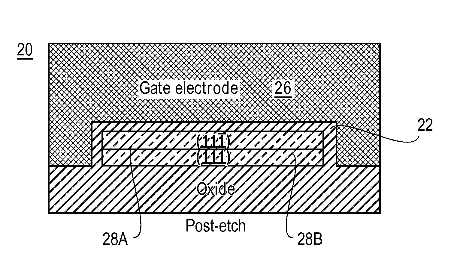
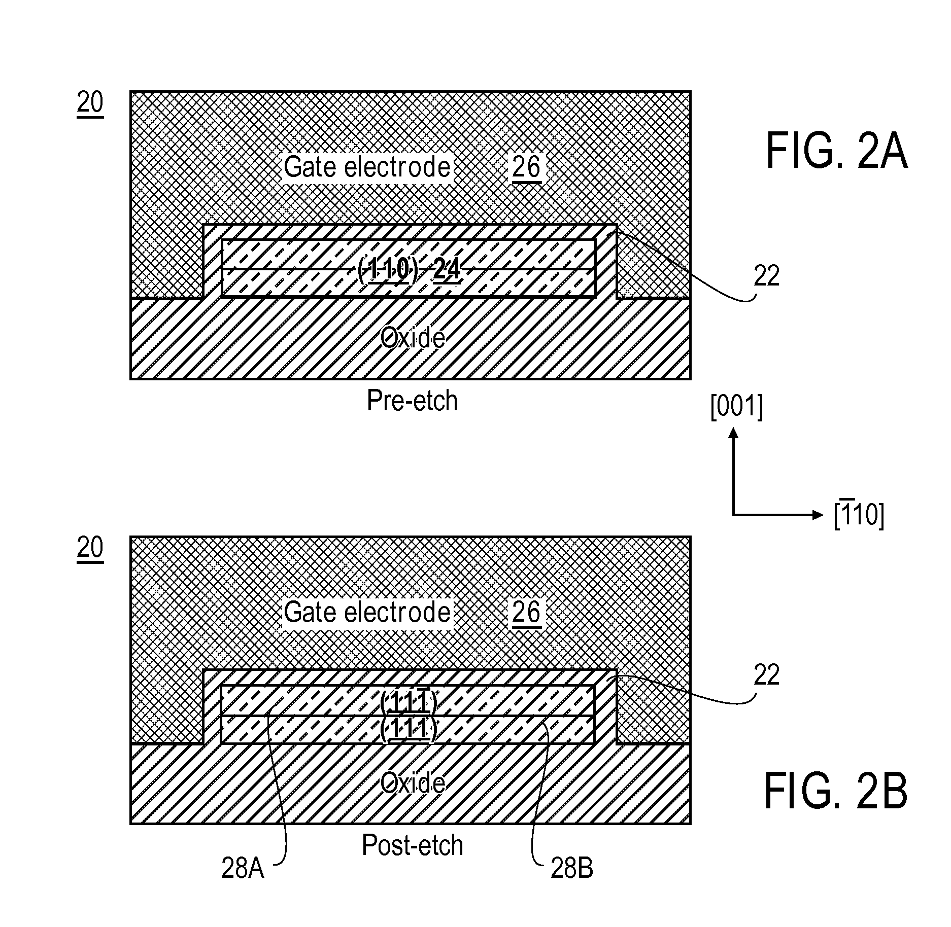
[0034]Described herein are devices in which the interface between a semiconductor channel and a source / drain (S / D) in the vicinity of the inversion layer is characterized by being made of more than one facet of a family of equivalent lattice planes. The S / D material can be made of a semiconducting material or of a metal. In both cases, the interface can have a thin passivation layer. Although such devices will be discussed with reference to certain illustrated examples thereof, the present invention is not intended to be limited through presentation of these examples. Instead, the invention is defined in the claims following this description and the examples presented herein are intended only to help illustrate features of the invention in a non-limiting fashion. We start by describing a FET where the S / D material is a metal.

[0035]Metal S / D FETs in which a surface of a semiconductor channel proximate to the metal S / D is formed of two or more of a family of equivalent lattice planes ...


PUM


Abstract

FET configurations in which two (or more) facets are exposed on a surface of a semiconductor channel, the facets being angled with respect to the direction of the channel, allow for conformal deposition of a convex or concave S / D. A convex tip of the S / D enhances electric fields at the interface, reducing the resistance between the S / D and the channel. In contrast, a S / D having a concave tip yields a dual-gate FET that emphasizes reduced short-channel effects rather than electric field enhancement. The use of self-limiting, selective wet etches to expose the facets facilitates process control, control of interface chemistry, and manufacturability.

Description

RELATED APPLICATION[0001]This application is a NONPROVISIONAL of and claims priority to U.S. Provisional Patent Application No. 61 / 097,209, filed 15 Sep. 2008, incorporated herein by reference.FIELD OF THE INVENTION[0002]The present invention relates to field effect transistors (FETs) having a source and / or drain (S / D), wherein a surface of a semiconductor channel proximate to the S / D is formed of two or more well-defined crystallographic surfaces of a common orientation, i.e., belonging to a family of equivalent lattice planes, that meet at an angle such that a surface of the S / D proximate to the semiconductor channel forms an angled feature.BACKGROUND[0003]Metal S / D FETs promise to improve the scalability, variability, and performance of ultra-thin-body complementary metal oxide semiconductor (CMOS) devices. There are two basic types of metal S / D devices. In the more traditional design, a relatively large Schottky barrier (ΦB) at the source is used to control the net rate of carri...

Claims


Application Information

Patent Timeline
Patent Type & Authority Patents(United States)
IPC IPC(8): H01L29/04
CPCH01L29/045H01L29/785H01L29/78606H01L29/78648
Inventor GOEBEL, ANDREASCLIFTON, PAUL A.CONNELLY, DANIEL J.UKIRDE, VAISHALI
Owner ACORN SEMI LLC
Why Eureka
Try Eureka