Using storage cells to perform computation

a technology of storage cells and computation, applied in the field of memory cells, can solve the problem that the speed of buses has not increased at an equal pa

Active Publication Date: 2012-08-07
GSI TECH
View PDF6 Cites 454 Cited by
  • Summary
  • Abstract
  • Description
  • Claims
  • Application Information

AI Technical Summary

Problems solved by technology

Unfortunately, while CPU speeds have increased tremendously in recent years, the bus speeds have not increased at an equal pace.

Method used


Image

  • Using storage cells to perform computation
  • Using storage cells to perform computation
  • Using storage cells to perform computation

Examples


Embodiment Construction

[0032]In the following detailed description, numerous specific details are set forth in order to provide a thorough understanding of the invention. However, it will be understood by those skilled in the art that the present invention may be practiced without these specific details. In other instances, well-known methods, procedures, and components have not been described in detail so as not to obscure the present invention.

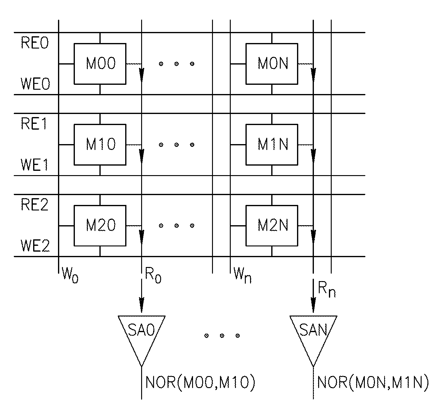
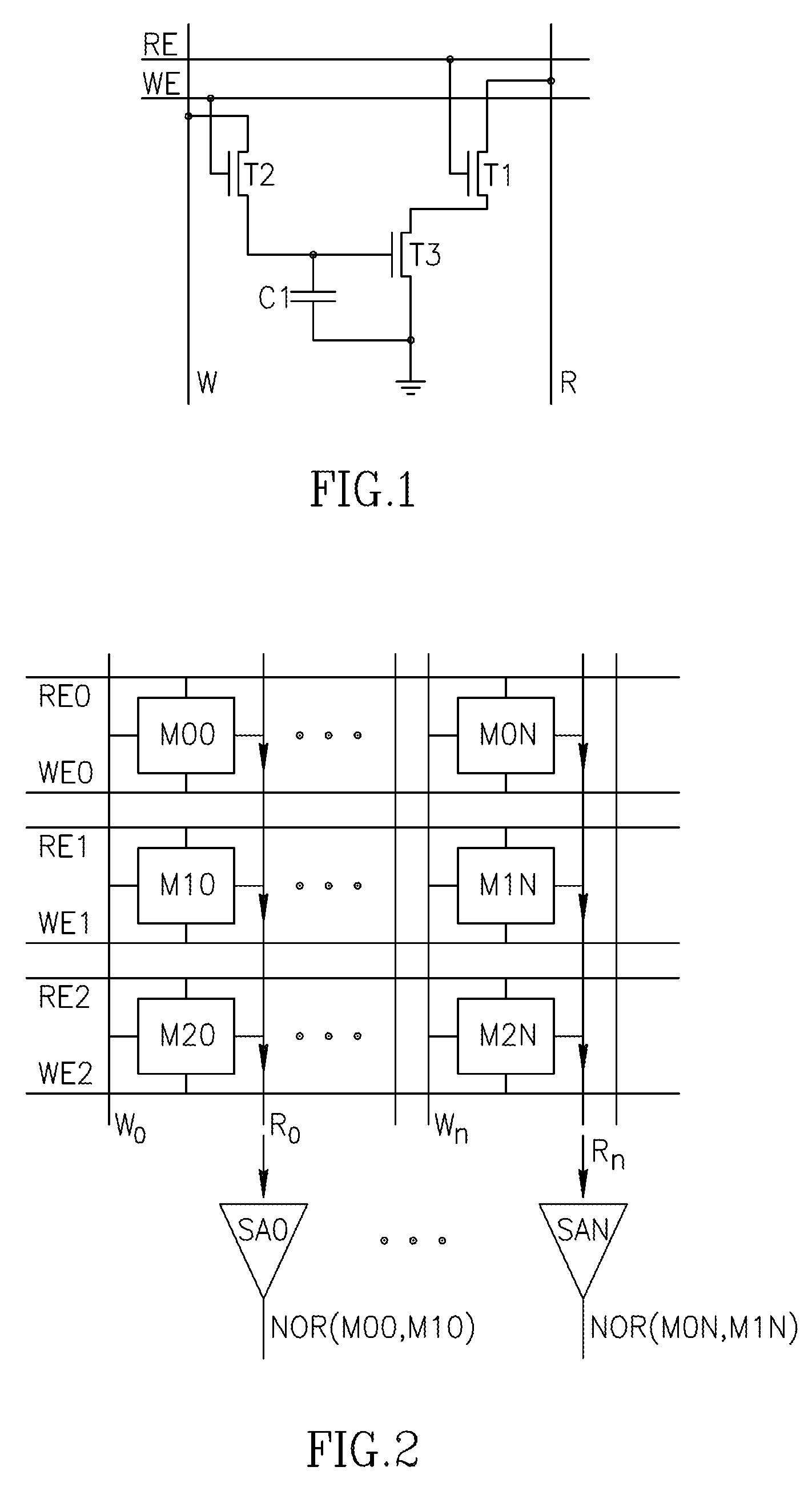
[0033]Applicants have realized that computing operations may be performable within the memory array. As an illustration, FIG. 1 illustrates a standard 3T DRAM memory cell, formed of three transistors, T1, T2, T3 and a capacitor C1. The input to transistor T1 is connected to a read (R) line while its gate is connected to a read enable (RE) or a word line. The input to transistor T3 is connected to the output of transistor T1 while its gate is connected to the output of transistor T2, which is the input to capacitor C1. The output of transistor T2 is connected both ...


PUM


Abstract

An in-memory processor includes a memory array which stores data and an activation unit to activate at least two cells in a column of the memory array at generally the same time thereby to generate a Boolean function output of the data of the at least two cells. Another embodiment shows a content addressable memory (CAM) unit without any in-cell comparator circuitry.

Description

FIELD OF THE INVENTION[0001]The present invention relates to memory cells generally and to their use for computation in particular.BACKGROUND OF THE INVENTION[0002]Memory arrays, which store large amounts of data, are known in the art. Over the years, manufacturers and designers have worked to make the arrays physically smaller but the amount of data stored therein larger.[0003]Computing devices typically have one or more memory array to store data and a central processing unit (CPU) and other hardware to process the data. The CPU is typically connected to the memory array via a bus. Unfortunately, while CPU speeds have increased tremendously in recent years, the bus speeds have not increased at an equal pace. Accordingly, the bus connection acts as a bottleneck to increased speed of operation.SUMMARY OF THE PRESENT INVENTION[0004]There is provided, in accordance with a preferred embodiment of the present invention, a NOR device including a plurality of memory cells which store data...

Claims


Application Information

Patent Timeline
Patent Type & Authority Patents(United States)
IPC IPC(8): G11C7/00G11C7/22
CPCG11C29/34G11C15/043G11C7/1006
Inventor AKERIB, AVIDANAGAM, ORENEHRMAN, ELIMEYASSED, MOSHE
Owner GSI TECH
Why Eureka
Try Eureka