Method for manufacturing electronic device

a manufacturing method and electronic technology, applied in the direction of contact member manufacturing, conductive pattern formation, printed circuit aspects, etc., can solve the problems of troublesome reinforcement material, inconvenient drilling and punching treatment, and high cost of laser beam use, so as to achieve easy formation, high accuracy, and control the shape and size of the opening.

Inactive Publication Date: 2012-08-14
SEMICON ENERGY LAB CO LTD
View PDF40 Cites 90 Cited by
  • Summary
  • Abstract
  • Description
  • Claims
  • Application Information

AI Technical Summary

Benefits of technology

[0012]By using a prepreg including a reinforcing material as a sealing film, an electronic element can be sealed with a resin film including the reinforcing material; therefore, the strength of the electronic element can be increased. Meanwhile, in the case where an opening is formed in the sealing film in order to expose an extraction terminal of an electronic element, the reinforcing material is also needed to be removed with the resin film. The reinforcing material is troublesome when the opening is formed in the resin film.
[0018]According to this embodiment, an opening can be easily formed with high accuracy in an insulating film formed by curing a prepreg including a reinforcing material, with the use of a means other than laser beam irradiation. This is because according to this embodiment, the position where an opening is formed can be determined in a self-aligned manner depending on the position where a protrusion is formed, and the accuracy of the position where an opening is formed can be ensured by the accuracy of the position where the protrusion is formed and the shape and size of the opening can be controlled by changing the height and shape of the protrusion. Therefore, in the step of forming the opening, highly accurate alignment like determination of a position where laser beam irradiation is performed is not necessary.
[0022]Thus, in the method for manufacturing an electronic device, according to the above embodiment, as described above, an opening can be easily formed with high accuracy in an insulating film formed by curing a prepreg including a reinforcing material, with the use of a means other than laser beam irradiation.
[0025]In a method for manufacturing an electronic device, according to an embodiment of the present invention, the accuracy of the position where the opening is formed in an insulating film (cured prepreg) including a reinforcing material is ensured in a self-aligned manner by the accuracy of the position where a protrusion is formed and the shape and size of the opening can be controlled by changing the height and shape of the protrusion. Therefore, by applying this embodiment, an opening can be easily formed in an insulating film including a reinforcing material with high accuracy, with the use of a means other than laser beam irradiation.

Problems solved by technology

The reinforcing material is troublesome when the opening is formed in the resin film.
For formation of an opening in a resin layer with which an electronic element is sealed, drill treatment and punching treatment are not suitable.
However, the step of forming an opening with the use of a laser beam takes much time and needs a skill because it is difficult to determine whether both the resin film and the reinforcing material are removed.
Thus, depending on the skill of an operator, the resin film and / or the reinforcing material might be insufficiently removed and thus the areas of regions exposed in openings might vary.
Accordingly, the values of connection resistance of two conductors electrically connected through an opening vary, which makes it difficult to manufacture an electric element having electric characteristics with a designed value.
In addition, in the case of employing the step of forming an opening with the use of a laser beam, a mechanical impact on an electronic element is small as compared to drilling or a punching; however, the possibility that performance of the electronic element is degraded by energy of a laser beam cannot be completely eliminated.

Method used


Image

  • Method for manufacturing electronic device
  • Method for manufacturing electronic device
  • Method for manufacturing electronic device

Examples


embodiment 1

[0049]In this embodiment, a terminal structure covered with n insulating film formed from a cured prepreg which includes a reinforcing material or cured resin film and a method for manufacturing the terminal structure will be described. Further, in this embodiment, an electronic device provided with a terminal having such a structure and a method for manufacturing the electronic device will also be described.

Terminal Structure

[0050]The terminal structure of this embodiment includes a conductor, a resin film including a reinforcing material and covering the conductor, and an opening formed in a region of the resin film, which overlaps with the conductor. In this opening, the conductor is exposed at a surface of the resin film and thus, the conductor can be electrically connected to another conductor.

Description of Insulating Surface

[0051]In the terminal structure, a first conductor is formed over an insulating surface, for example. As the insulating surface, for example, a surface of...

embodiment 2

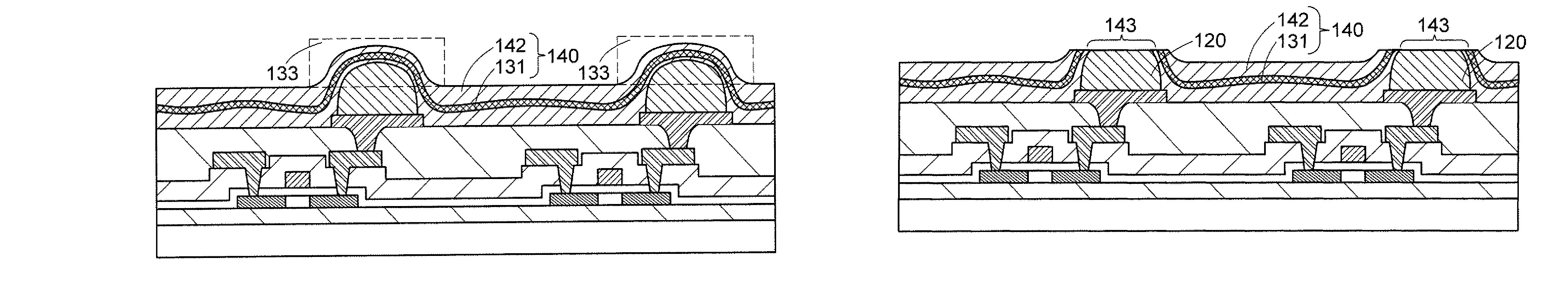
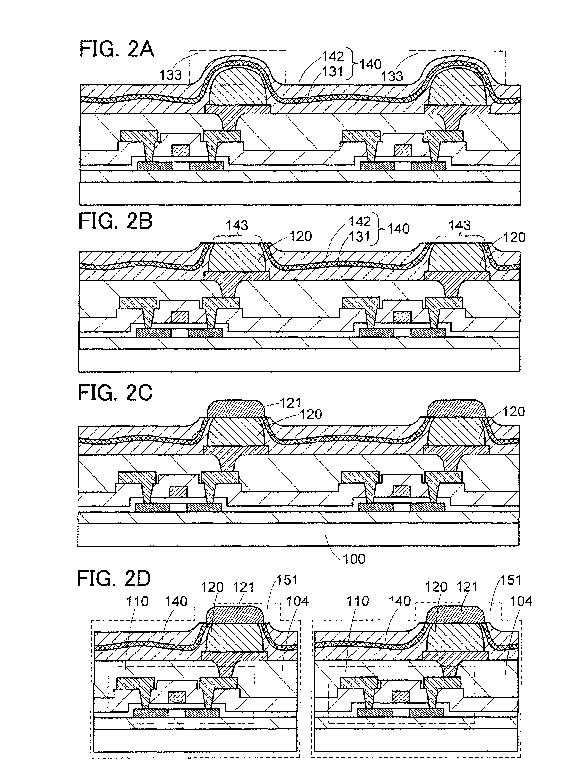
[0097]In this embodiment, the step of forming the openings 143 in the insulating film 140 (see FIG. 2B) will be described. FIG. 6 and FIG. 7 are views illustrating examples of structures of grinding machines. The grinding machines in FIG. 6 and FIG. 7 make it possible to preferentially remove a protruding portion of a top surface of the insulating film 140.

example 1

[Structure Example 1 of Grinding Machine and Grinding Step]

[0098]Hereinafter, a structure of a grinding machine 201 in FIG. 6 and how to use the grinding machine 201 in the step in FIG. 2B will be described.

[0099]As illustrated in FIG. 6, the grinding machine 201 includes a grinding surface plate 210 having a grinding surface, a rotating unit 211 which rotates the grinding surface plate 210, a substrate holding unit 212 which holds a processing substrate 200, a rotating unit 213 which rotates the substrate holding unit 212, and a nozzle 215 which supplies liquid 214 to the grinding surface. For example, a sucking chuck can be applied to the substrate holding unit 212 and pure water, slurry, or the like can be used as the liquid 214.

[0100]To perform the step in FIG. 2B, first, the processing substrate 200 which has been subjected to the steps up to and including the step in FIG. 2A is fixed to the substrate holding unit 212. The processing substrate 200 is fixed to the substrate hold...


PUM

PropertyMeasurementUnit
thicknessaaaaaaaaaa
thicknessaaaaaaaaaa
lengthaaaaaaaaaa

Abstract

To provide a method for forming an opening with high accuracy in an insulating film obtained by curing a prepreg including a reinforcing material in a step of exposing a terminal portion sealed with the insulating film, with the use of a means other than laser beam irradiation. A protrusion is formed using a conductor. An uncured prepreg including a reinforcing material is closely attached to the protrusion and the prepreg is cured, so that an insulating film including the reinforcing material is formed. A portion of a top surface of the insulating film protrudes due to the protrusion. The protruding portion is preferentially removed together with the reinforcing material to form an opening in the insulating film by grinding treatment or the like, so that an opening which exposes the protrusion is formed in the insulating film.

Description

BACKGROUND OF THE INVENTION[0001]1. Field of the Invention[0002]In this specification, a terminal structure including a conductor covered with an insulating film will be described. Further, an electronic device provided with a terminal having such a structure will also be described.[0003]2. Description of the Related Art[0004]A resin layer formed by curing a prepreg including a reinforcing material such as a glass fiber or a glass filler is applied to a support, an insulating film, a protective material, or the like of a printed wiring board, an electronic device, or the like (for example, see Patent Documents 1 to 4). Since a multilayer wiring is formed, an opening penetrating a resin layer formed using a prepreg is formed in this layer in order to form an electrical connection portion with the external.[0005]For example, Patent Document 1 discloses that an insulating layer of a printed wiring board is formed using a prepreg and an opening is formed in the insulating layer with las...

Claims


Application Information

Patent Timeline
Patent Type & Authority Patents(United States)
IPC IPC(8): H05K3/36
CPCH01L21/6836H01L23/3164H01L24/03H01L24/05H01L24/11H05K3/4007H01L23/3114H01L23/5389H01L24/13H01L24/16H01L2221/6834H01L2224/05624H01L2224/05639H01L2224/05644H01L2224/05647H01L2224/05655H01L2224/05666H01L2224/05669H01L2224/05671H01L2224/0568H01L2224/05681H01L2224/05684H01L2224/11002H01L2224/13099H01L2224/16H01L2924/01004H01L2924/01013H01L2924/01014H01L2924/01022H01L2924/01027H01L2924/01029H01L2924/0103H01L2924/01032H01L2924/01033H01L2924/01042H01L2924/01046H01L2924/01047H01L2924/01049H01L2924/0106H01L2924/01073H01L2924/01074H01L2924/01078H01L2924/01079H01L2924/01082H01L2924/014H01L2924/04941H01L2924/19041H01L2924/30105H05K3/045H05K3/281H05K2201/0367H01L2924/01005H01L2924/01006H01L2924/01024H01L2924/01041H01L2924/01072H01L2924/01076H01L2224/13139H01L2224/136H01L2924/0001H01L2224/0401Y10T29/49155Y10T29/4913Y10T29/49165Y10T29/49126Y10T29/49204Y10T29/49117H01L2924/00014H01L2924/15787H01L2924/15788H01L2924/181H01L2924/14H01L2924/00
Inventor HAMATANI, TOSHIJIFUKUTOME, TAKAHIRO
Owner SEMICON ENERGY LAB CO LTD
Why Eureka
Try Eureka