Axiocentric scrubbing land grid array contacts and methods for fabrication

a grid array and contact technology, applied in the field of electrical contact structures, can solve problems such as negative affecting the mating of electrical contacts on each

Active Publication Date: 2012-09-11
GLOBALFOUNDRIES US INC
View PDF38 Cites 14 Cited by
  • Summary
  • Abstract
  • Description
  • Claims
  • Application Information

AI Technical Summary

Benefits of technology

[0009]In another aspect of the invention, a method for manufacturing a contact structure for microelectronics manufacturing comprises: providing a carrier element defining a first opening therethrough; positioning a molded element on opposite sides of the carrier element by passing the molded element partially through the first opening; coating the molded element with an electrically conductive material; fabricating a helix shaped contact from the electrically conductive material on the opposite sides of the carrier element, the helix shaped contact being positioned over the molded element, the helix shaped contact having a first portion and a second portion on the opposing sides of the carrier element, respectively, and the first and second portions being in mirror image relationship to each other; heating the combined helix shaped contact and the molded element such that the molded element is ablated and the helix shaped contact substantially retains the shape of the molded element.

Problems solved by technology

However, decreasing the size of contact structures negatively affects mating of electrical contacts on each of the electrical devices being pressed together.

Method used


Image

  • Axiocentric scrubbing land grid array contacts and methods for fabrication
  • Axiocentric scrubbing land grid array contacts and methods for fabrication
  • Axiocentric scrubbing land grid array contacts and methods for fabrication

Examples


Embodiment Construction

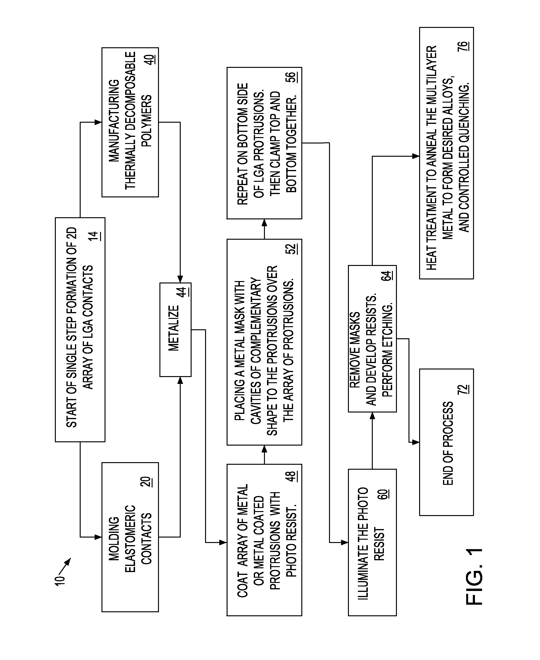
[0030]Referring to FIG. 1, a method 10 according to one embodiment of the present invention includes the general steps below including step 14 forming a substrate with a 2d array of vias (for example, conducting vias) as a first step to forming a 2d array of contacts. Two different alternatives can be pursued after step 14, a first path is to manufacture contacts shaped from thermally decomposable polymers in step 40. Contact elements are shaped from thermally decomposable polymers, and the sacrificial polymers are molded into a carrier plane with vias. The plurality of contact may be formed in an array of contacts having a pattern.

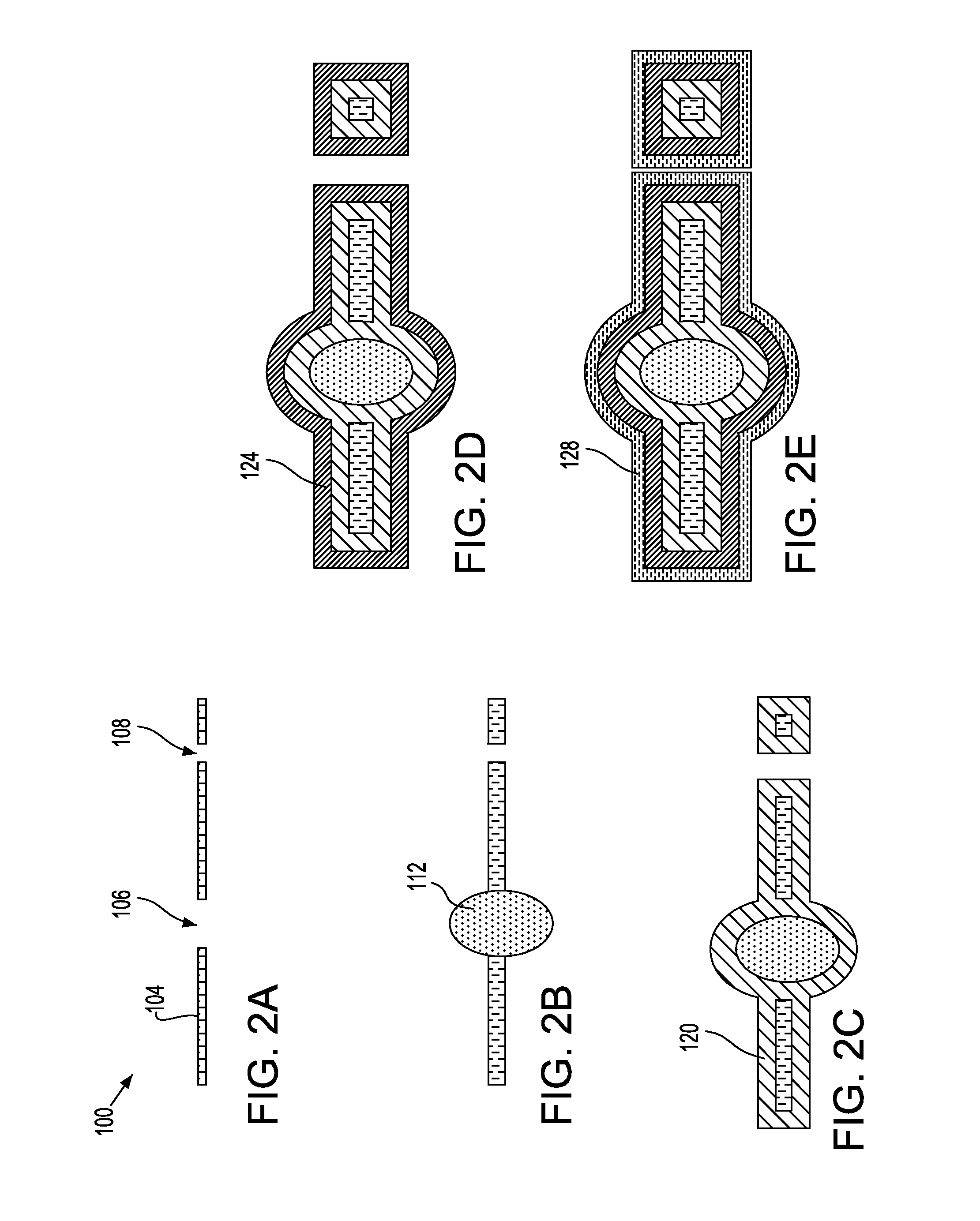
[0031]A second path is to mold elastomeric contact elements into a carrier plane in step 20. After either steps 20 or 40, the contact elements are metalized using known methods in step 44. Both paths continue in step 48 wherein the protruding contact elements are coated with metal layers and photo resist. A conformally coating resist such as electrophoret...


PUM

PropertyMeasurementUnit
thickaaaaaaaaaa
thickaaaaaaaaaa
frequencyaaaaaaaaaa

Abstract

A contact structure and assembly and a method for manufacturing the same for a microelectronics device includes first and second electrically conductive contacts being helically shaped. A carrier element is attached to and positioned between the first and second contacts. The first and second contacts are in electrical communication with each other, and the first and second contacts are in a mirror image relationship with each other. A pair of insulating substrates each include electrically conductive members. A contact point on each of the first and second contacts is attached and electrically communicating to respective electrically conductive members such that the first and second electrically conductive contacts between the pair of insulating substrates form an electrically conductive package. A metal layer on the carrier element provides electrical conductivity through a first opening defined by the carrier element between the first and second portions of the helix shaped contact.

Description

STATEMENT REGARDING FEDERALLY SPONSORED RESEARCH OF DEVELOPMENT[0001]This invention was made with Government support under Contract No.: HR0011-07-9-0002 awarded by (DARPA) Defense Advanced Research Projects Agency. The Government has certain rights in this invention.CROSS REFERENCE TO RELATED APPLICATIONS[0002]This application is related to the following commonly-owned, co-pending United States Patent Application filed on even date herewith, the entire contents and disclosure of which is expressly incorporated by reference herein in its entirety: U.S. patent application Ser. No. (12 / 614,231), for “Metallurgical Clamshell Methods for Micro Land Grid Array Fabrication”.BACKGROUND[0003]The present invention relates generally to the electrical contact structures in the field of microelectronics, and more particularly, relates to electrical contact structures and a method for manufacturing the same for microelectronics and semiconductor manufacturing.[0004]Typical Land Grid Array (LGA) ...

Claims


Application Information

Patent Timeline
Patent Type & Authority Patents(United States)
IPC IPC(8): H05K1/11
CPCH01R12/7082H01R12/714H05K3/4092H01R13/2414H01R13/2421Y10T29/49224H05K2201/0311H05K2201/10265H05K2201/10378H05K3/326Y10T29/49226H05K1/11H01R43/16
Inventor HOUGHAM, GARETHMCVICKER, GERARDGU, XIAOXIONGKANG, SUNG K.LIBSCH, FRANK R.LIU, XIAO H.
Owner GLOBALFOUNDRIES US INC
Why Eureka
Try Eureka