Avalanche capability improvement in power semiconductor devices

a technology of power semiconductor devices and avalanche capability, which is applied in the direction of semiconductor devices, solid-state devices, transistors, etc., can solve the problems of weakening the avalanche capability of trench mosfet, hazardous condition of power semiconductor devices, and limited poor avalanche capability discussed abov

Active Publication Date: 2012-09-11
FORCE MOS TECH CO LTD
View PDF25 Cites 3 Cited by
  • Summary
  • Abstract
  • Description
  • Claims
  • Application Information

AI Technical Summary

Benefits of technology

[0007]The present invention has been conceived to solve the above-described problems with the related art, and it is an object of the invention to provide a technique which makes it possible to avoid the avalanche occurring near bottom of the trenched gates and to prevent the parasitic bipolar transistor from turning-on.
[0015]According to a seventh aspect of the present invention, there is provided a power semiconductor device comprising a plurality of trench MOSFETs wherein each said source-body contact trench has sidewalls with taper angle α1 within said source region, and has sidewalls with taper angle α2 in said body region with respect to top surface of said epitaxial layer, wherein said taper angle α1 is equal to or less than 90 degree and equal to or greater than said taper angle α2. By employing this structure with said taper angle α2 is less than 90 degree, the area of said body ohmic contact doped region is enlarged surrounding not only bottom but also sidewall of each said source-body contact trench, thus further enhancing UIS performance.

Problems solved by technology

The conventional structure in FIG. 1 is accoutering a technical difficulty which is that avalanche always occurs near bottom of said trenched gates 110, causing a hazardous condition to the power semiconductor device.
Therefore, said parasitic bipolar transistor is easily to be triggered turning on due to the high resistance Rb, thus weakening the avalanche capability of the trench MOSFET.
However, the limitation of poor avalanche capability discussed above is still pronounced in this structure due to the easily turning-on of a parasitic bipolar transistor and the occurring of avalanche near bottom of said trenched gates 130.
For other power semiconductor power device, for example trench IGBTs, the same disadvantage of poor avalanche capability is also affecting the performance of the power semiconductor device.

Method used


Image

  • Avalanche capability improvement in power semiconductor devices
  • Avalanche capability improvement in power semiconductor devices
  • Avalanche capability improvement in power semiconductor devices

Examples


Embodiment Construction

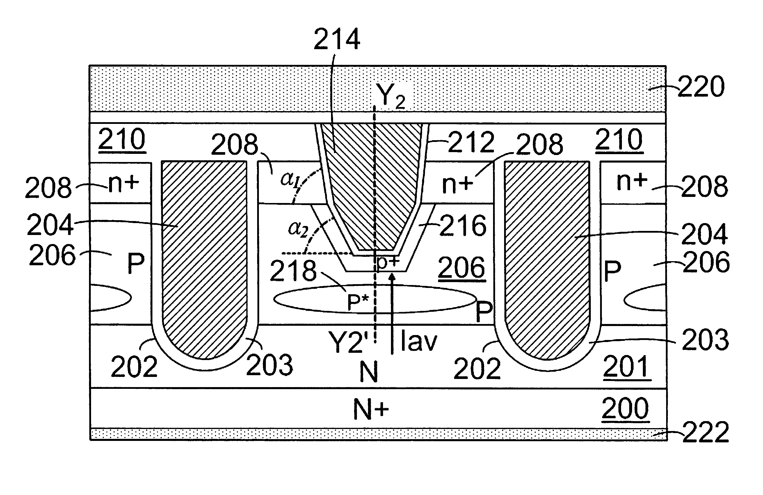
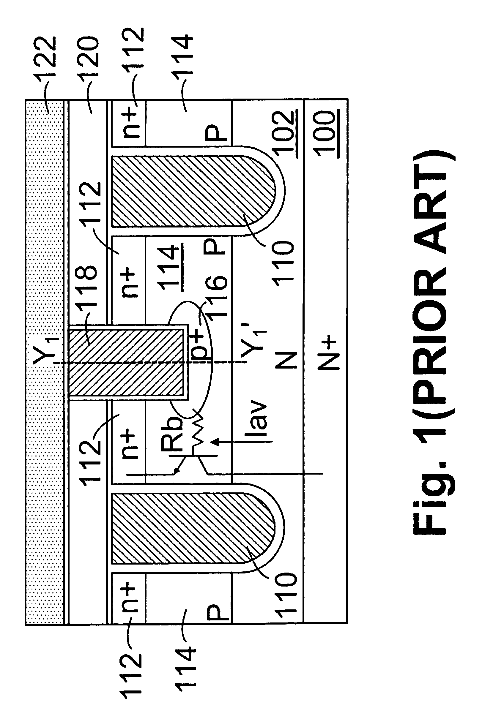
[0047]Please refer to FIG. 4 for a cross sectional-view of a preferred N-channel trench MOSFET which formed on an N+ substrate 200 with back metal 222 of Ti / Ni / Ag on rear side as drain electrode. Onto said N+ substrate 200, a lighter doped N epitaxial layer 201 is grown, and a plurality of trenched gates are formed therein. The trenched gates further comprises: a plurality of gate trenches 202; a gate oxide layer 203 lining the inner surface of each of said gate trenches 202; a doped poly-silicon layer 204 filled in each of said gate trenches, wherein the top surface of said doped poly-silicon layer 204 not higher than sidewalls of said gate trenches. The preferred N-channel trench MOSFET further comprises: P body regions 206 formed in upper portion of said N epitaxial layer 201 and extending between every two adjacent of said gate trenches 202; n+ source regions 208 near top surface of said P body regions 206 and surrounding the sidewalls of said gate trenches 202; an insulation la...


PUM


Abstract

A power semiconductor device with improved avalanche capability structures is disclosed. By forming at least an avalanche capability enhancement doped regions with opposite conductivity type to epitaxial layer underneath an ohmic contact doped region which surrounds at least bottom of trenched contact filled with metal plug between two adjacent gate trenches, avalanche current is enhanced with the disclosed structures.

Description

FIELD OF THE INVENTION[0001]This invention related generally to the cell structure and device configuration of power semiconductor devices. More particularly, this invention relates to power semiconductor devices with improved avalanche capability.BACKGROUND OF THE INVENTION[0002]In U.S. Pat. No. 6,888,196, a conventional structure of power semiconductor device is disclosed, as shown in FIG. 1, wherein an N-channel trench MOSFET comprising a plurality of trenched gates 110 surrounded by n+ source regions 112 encompassed in P body regions 114 is formed in an N epitaxial layer 102 over an N+ substrate 100. To connect said source regions 112 and said body regions 114 to a source metal 122, a trenched source-body contact 118 with vertical sidewall is employed penetrating through a contact interlayer 120, said n+ source regions 112 and extending into said P body regions 114. Furthermore, a p+ body ohmic contact doped region 116 is implanted surrounding bottom of said trenched source-body...

Claims


Application Information

Patent Timeline
Patent Type & Authority Patents(United States)
IPC IPC(8): H01L29/76H01L31/119H01L31/113H01L31/062H01L29/94
CPCH01L29/0626H01L29/1095H01L29/41766H01L29/66727H01L29/66734H01L29/7397H01L29/7808H01L29/7813H01L29/4236H01L29/456
Inventor HSIEH, FU-YUAN
Owner FORCE MOS TECH CO LTD
Why Eureka
Try Eureka